- 您现在的位置:买卖IC网 > PDF目录16848 > AD9523-1/PCBZ (Analog Devices Inc)BOARD EVAL FOR AD9523-1 PDF资料下载
参数资料
| 型号: | AD9523-1/PCBZ |
| 厂商: | Analog Devices Inc |
| 文件页数: | 41/60页 |
| 文件大小: | 0K |
| 描述: | BOARD EVAL FOR AD9523-1 |
| 设计资源: | AD9523(-1) Eval Board Schematic AD9523(-1) BOM AD9523(-1) Gerber Files |
| 标准包装: | 1 |
| 主要目的: | 计时,时钟发生器 |
| 嵌入式: | 否 |
| 已用 IC / 零件: | AD9523 |
| 主要属性: | 板载 PLL 环路滤波器 |
| 次要属性: | LED 状态指示器 |
| 已供物品: | 板 |
第1页第2页第3页第4页第5页第6页第7页第8页第9页第10页第11页第12页第13页第14页第15页第16页第17页第18页第19页第20页第21页第22页第23页第24页第25页第26页第27页第28页第29页第30页第31页第32页第33页第34页第35页第36页第37页第38页第39页第40页当前第41页第42页第43页第44页第45页第46页第47页第48页第49页第50页第51页第52页第53页第54页第55页第56页第57页第58页第59页第60页
AD9523-1
Rev. B | Page 46 of 60
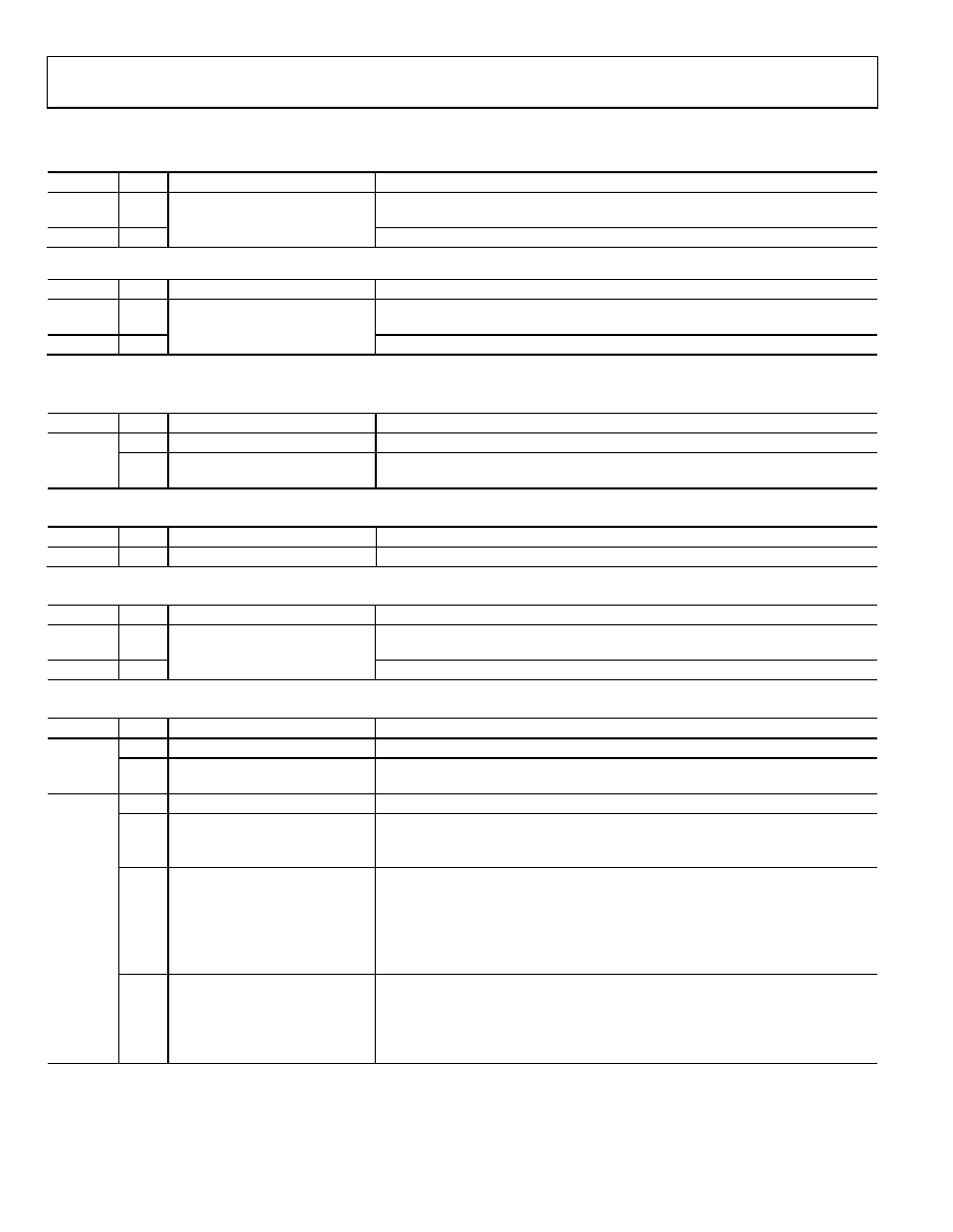
Input PLL (PLL1) (Address 0x010 to Address 0x01D)
Table 34. PLL1 REFA R Divider Control
Address
Bits
Bit Name
Description
0x010
[7:0]
REFA R divider
10-bit REFA R divider, Bits[7:0] (LSB). Divide-by-1 to divide-by-1023.
00000000, 00000001: divide-by-1.
0x011
[1:0]
10-bit REFA R divider, Bits[9:8] (MSB).
Table 35. PLL1 REFB R Divider Control1
Address
Bits
Bit Name
Description
0x012
[7:0]
REFB R divider
10-bit REFB R divider, Bits[7:0] (LSB). Divide-by-1 to divide-by-1023.
00000000, 00000001: divide-by-1.
0x013
[1:0]
10-bit REFB R divider, Bits[9:8] (MSB).
1 Requires Register 0x01C, Bit 7 = 1 for division that is independent of REFA division.
Table 36. PLL1 Reference Test Divider
Address
Bits
Bit Name
Description
[7:6]
Reserved
Reserved.
0x014
[5:0]
REF_TEST divider
6-bit reference test divider. Divide-by-1 to divide-by-63.
000000, 000001: divide-by-1.
Table 37. PLL1 Reserved
Address
Bits
Bit Name
Description
0x015
[7:0]
Reserved
Reserved.
Table 38. PLL1 Feedback N Divider Control
Address
Bits
Bit Name
Description
0x016
[7:0]
10-bit feedback divider, Bits[7:0] (LSB). Divide-by-1 to divide-by-1023.
00000000, 00000001: divide-by-1.
0x017
[1:0]
PLL1 feedback N divider control
(N_PLL1)
10-bit feedback divider, Bits[1:0] (MSB).
Table 39. PLL1 Charge Pump Control
Address
Bits
Bit Name
Description
7
PLL1 charge pump tristate
Tristates the PLL1 charge pump.
0x018
[6:0]
PLL1 charge pump control
These bits set the magnitude of the PLL1 charge pump current. Granularity is ~0.5 μA
with a full-scale magnitude of ~63.5 μA.
[7:5]
Reserved
Reserved.
4
Enable SPI control of antibacklash
pulse width
Controls the functionality of Register 0x019, Bits[3:2].
0 (default): the device automatically controls the antibacklash period.
1: antibacklash period defined by Register 0x019, Bits[3:2].
[3:2]
Antibacklash pulse width control
Controls the PFD antibacklash period.
00 (default): minimum.
01: low.
10: high.
11: maximum.
These bits are ineffective unless Register 0x019, Bit 4 = 1.
0x019
[1:0]
PLL1 charge pump mode
Controls the mode of the PLL1 charge pump.
00: tristate.
01: pump up.
10: pump down.
11 (default): normal.
相关PDF资料 |
PDF描述 |
|---|---|
| V150C5C100BF | CONVERTER MOD DC/DC 5V 100W |
| V150C5C100BL3 | CONVERTER MOD DC/DC 5V 100W |
| V150C5C100B3 | CONVERTER MOD DC/DC 5V 100W |
| V150C5C100B2 | CONVERTER MOD DC/DC 5V 100W |
| AD9512/PCBZ | BOARD EVAL FOR AD9512 |
相关代理商/技术参数 |
参数描述 |
|---|---|
| AD9523BCPZ | 功能描述:IC INTEGER-N CLCK GEN 72LFCSP RoHS:是 类别:集成电路 (IC) >> 时钟/计时 - 专用 系列:- 标准包装:28 系列:- 类型:时钟/频率发生器 PLL:是 主要目的:Intel CPU 服务器 输入:时钟 输出:LVCMOS 电路数:1 比率 - 输入:输出:3:22 差分 - 输入:输出:无/是 频率 - 最大:400MHz 电源电压:3.135 V ~ 3.465 V 工作温度:0°C ~ 85°C 安装类型:表面贴装 封装/外壳:64-TFSOP (0.240",6.10mm 宽) 供应商设备封装:64-TSSOP 包装:管件 |
| AD9523BCPZ-REEL7 | 功能描述:IC INTEGER-N CLCK GEN 72LFCSP RoHS:是 类别:集成电路 (IC) >> 时钟/计时 - 专用 系列:- 标准包装:28 系列:- 类型:时钟/频率发生器 PLL:是 主要目的:Intel CPU 服务器 输入:时钟 输出:LVCMOS 电路数:1 比率 - 输入:输出:3:22 差分 - 输入:输出:无/是 频率 - 最大:400MHz 电源电压:3.135 V ~ 3.465 V 工作温度:0°C ~ 85°C 安装类型:表面贴装 封装/外壳:64-TFSOP (0.240",6.10mm 宽) 供应商设备封装:64-TSSOP 包装:管件 |
| AD9524 | 制造商:AD 制造商全称:Analog Devices 功能描述:Jitter Cleaner and Clock Generator with 6 Differential or 13 LVCMOS Outputs |
| AD9524/PCBZ | 功能描述:BOARD EVAL FOR AD9524 RoHS:是 类别:编程器,开发系统 >> 评估演示板和套件 系列:- 标准包装:1 系列:PSoC® 主要目的:电源管理,热管理 嵌入式:- 已用 IC / 零件:- 主要属性:- 次要属性:- 已供物品:板,CD,电源 |
| AD9524BCPZ | 功能描述:IC INTEGER-N CLCK GEN 48LFCSP RoHS:是 类别:集成电路 (IC) >> 时钟/计时 - 专用 系列:- 标准包装:28 系列:- 类型:时钟/频率发生器 PLL:是 主要目的:Intel CPU 服务器 输入:时钟 输出:LVCMOS 电路数:1 比率 - 输入:输出:3:22 差分 - 输入:输出:无/是 频率 - 最大:400MHz 电源电压:3.135 V ~ 3.465 V 工作温度:0°C ~ 85°C 安装类型:表面贴装 封装/外壳:64-TFSOP (0.240",6.10mm 宽) 供应商设备封装:64-TSSOP 包装:管件 |
发布紧急采购,3分钟左右您将得到回复。