- 您现在的位置:买卖IC网 > PDF目录16848 > AD9523-1/PCBZ (Analog Devices Inc)BOARD EVAL FOR AD9523-1 PDF资料下载
参数资料
| 型号: | AD9523-1/PCBZ |
| 厂商: | Analog Devices Inc |
| 文件页数: | 15/60页 |
| 文件大小: | 0K |
| 描述: | BOARD EVAL FOR AD9523-1 |
| 设计资源: | AD9523(-1) Eval Board Schematic AD9523(-1) BOM AD9523(-1) Gerber Files |
| 标准包装: | 1 |
| 主要目的: | 计时,时钟发生器 |
| 嵌入式: | 否 |
| 已用 IC / 零件: | AD9523 |
| 主要属性: | 板载 PLL 环路滤波器 |
| 次要属性: | LED 状态指示器 |
| 已供物品: | 板 |
第1页第2页第3页第4页第5页第6页第7页第8页第9页第10页第11页第12页第13页第14页当前第15页第16页第17页第18页第19页第20页第21页第22页第23页第24页第25页第26页第27页第28页第29页第30页第31页第32页第33页第34页第35页第36页第37页第38页第39页第40页第41页第42页第43页第44页第45页第46页第47页第48页第49页第50页第51页第52页第53页第54页第55页第56页第57页第58页第59页第60页
AD9523-1
Rev. B | Page 22 of 60
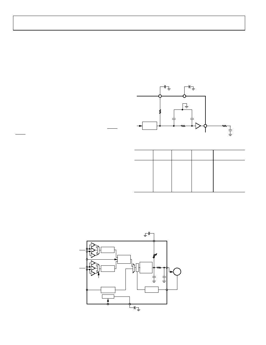
COMPONENT BLOCKS—INPUT PLL (PLL1)
PLL1 General Description
Fundamentally, the input PLL (referred to as PLL1) consists of
a phase-frequency detector (PFD), charge pump, passive loop filter,
and an external VCXO operating in a closed loop (see Figure 26).
PLL1 has the flexibility to operate with a loop bandwidth of
approximately 10 Hz to 100 Hz. This relatively narrow loop
bandwidth gives the AD9523-1 the ability to suppress jitter that
appears on the input references (REFA and REFB). The output
of PLL1 then becomes a low jitter phase-locked version of the
reference input system clock.
PLL1 Reference Clock Inputs
The AD9523-1 features two separate differential reference clock
inputs, REFA and REFB. These inputs can be configured to
operate in full differential mode or single-ended CMOS mode.
In differential mode, these pins are internally self-biased. If
REFA or REFB is driven single-ended, the unused side (REFA,
REFB) should be decoupled via a suitable capacitor to a quiet
ground.
shows the equivalent circuit of REFA or REFB.
It is possible to dc-couple to these inputs, but the dc operation
point should be set as specified in the
tables.
To operate either the REFA input or the REFB input in 3.3 V
CMOS mode, the user must set Bit 5 or Bit 6, respectively, in
Register 0x01A (see Table 40). The single-ended inputs can be
driven by either a dc-coupled CMOS level signal or an ac-coupled
sine wave or square wave.
The differential reference input receiver is powered down when
the differential reference input is not selected, or when the PLL
is powered down. The single-ended buffers power down when
the PLL is powered down, when their respective individual power-
down registers are set, or when the differential receiver is selected.
The REFB R divider uses the same value as the REFA R divider
unless Bit 7, the enable REFB R divider independent division
control bit in Register 0x01C, is programmed as shown in Table 42.
PLL1 Loop Filter
The PLL1 loop filter requires the connection of an external
capacitor from LF1_EXT_CAP (Pin 7) to ground. The value of the
external capacitor depends on the use of an external VCXO and
the configuration parameters, such as input clock rate and desired
bandwidth. Normally, a 0.3 μF capacitor allows the loop bandwidth
to range from 10 Hz to 100 Hz and ensures loop stability over
the intended operating parameters of the device (see Table 43 for
RZERO values).
RZERO
CPOLE1
RPOLE2
CPOLE2
CHARGE
PUMP
LF1_EXT_CAP
LDO_PLL1
BUFFER
1k
0.3F
OSC_CTRL
AD9523-1
09278-
022
Figure 25. PLL1 Loop Filter
Table 19. PLL1 Loop Filter Programmable Values
RZERO
(kΩ)
CPOLE1
(nF)
RPOLE2
(kΩ)
CPOLE2
(nF)
(μF)
883
1.5 fixed
165 fixed
0.337 fixed
0.3
677
341
135
10
External
1 External loop filter capacitor.
An external R-C low-pass filter should be used at the OSC_CTRL
output. The values shown in Figure 25 add an additional low-pass
pole at ~530 Hz. This R-C network filters the noise associated with
the OSC_CTRL buffer to achieve the best noise performance at the
1 kHz offset region.
RZERO
CPOLE1
RPOLE2
LF1_EXT_CAP
SWITCH-
OVER
CONTROL
REFA
REFB
REFA
REFB
REF_SEL
REF_TEST
DIVIDE-BY-
1, 2, ...1023
CHARGE
PUMP
7 BITS,
0.5A LSB
VDD3_PLL
LDO_PLL1
1.8V LDO
3.3V CMOS
OR 1.8V
DIFFERENTIAL
OSC_CTRL
OSC_IN
DIVIDE-BY-
1, 2, ...1023
DIVIDE-BY-
1, 2, ...1023
DIVIDE-BY-
1, 2, ...63
P
F
D
VCXO
CPOLE2
AD9523-1
092
78
-021
Figure 26. Input PLL (PLL1) Block Diagram
相关PDF资料 |
PDF描述 |
|---|---|
| V150C5C100BF | CONVERTER MOD DC/DC 5V 100W |
| V150C5C100BL3 | CONVERTER MOD DC/DC 5V 100W |
| V150C5C100B3 | CONVERTER MOD DC/DC 5V 100W |
| V150C5C100B2 | CONVERTER MOD DC/DC 5V 100W |
| AD9512/PCBZ | BOARD EVAL FOR AD9512 |
相关代理商/技术参数 |
参数描述 |
|---|---|
| AD9523BCPZ | 功能描述:IC INTEGER-N CLCK GEN 72LFCSP RoHS:是 类别:集成电路 (IC) >> 时钟/计时 - 专用 系列:- 标准包装:28 系列:- 类型:时钟/频率发生器 PLL:是 主要目的:Intel CPU 服务器 输入:时钟 输出:LVCMOS 电路数:1 比率 - 输入:输出:3:22 差分 - 输入:输出:无/是 频率 - 最大:400MHz 电源电压:3.135 V ~ 3.465 V 工作温度:0°C ~ 85°C 安装类型:表面贴装 封装/外壳:64-TFSOP (0.240",6.10mm 宽) 供应商设备封装:64-TSSOP 包装:管件 |
| AD9523BCPZ-REEL7 | 功能描述:IC INTEGER-N CLCK GEN 72LFCSP RoHS:是 类别:集成电路 (IC) >> 时钟/计时 - 专用 系列:- 标准包装:28 系列:- 类型:时钟/频率发生器 PLL:是 主要目的:Intel CPU 服务器 输入:时钟 输出:LVCMOS 电路数:1 比率 - 输入:输出:3:22 差分 - 输入:输出:无/是 频率 - 最大:400MHz 电源电压:3.135 V ~ 3.465 V 工作温度:0°C ~ 85°C 安装类型:表面贴装 封装/外壳:64-TFSOP (0.240",6.10mm 宽) 供应商设备封装:64-TSSOP 包装:管件 |
| AD9524 | 制造商:AD 制造商全称:Analog Devices 功能描述:Jitter Cleaner and Clock Generator with 6 Differential or 13 LVCMOS Outputs |
| AD9524/PCBZ | 功能描述:BOARD EVAL FOR AD9524 RoHS:是 类别:编程器,开发系统 >> 评估演示板和套件 系列:- 标准包装:1 系列:PSoC® 主要目的:电源管理,热管理 嵌入式:- 已用 IC / 零件:- 主要属性:- 次要属性:- 已供物品:板,CD,电源 |
| AD9524BCPZ | 功能描述:IC INTEGER-N CLCK GEN 48LFCSP RoHS:是 类别:集成电路 (IC) >> 时钟/计时 - 专用 系列:- 标准包装:28 系列:- 类型:时钟/频率发生器 PLL:是 主要目的:Intel CPU 服务器 输入:时钟 输出:LVCMOS 电路数:1 比率 - 输入:输出:3:22 差分 - 输入:输出:无/是 频率 - 最大:400MHz 电源电压:3.135 V ~ 3.465 V 工作温度:0°C ~ 85°C 安装类型:表面贴装 封装/外壳:64-TFSOP (0.240",6.10mm 宽) 供应商设备封装:64-TSSOP 包装:管件 |
发布紧急采购,3分钟左右您将得到回复。