- 您现在的位置:买卖IC网 > PDF目录1987 > AD9540BCPZ-REEL7 (Analog Devices Inc)IC CLOCK GEN/SYNTHESIZER 48LFCSP PDF资料下载
参数资料
| 型号: | AD9540BCPZ-REEL7 |
| 厂商: | Analog Devices Inc |
| 文件页数: | 15/32页 |
| 文件大小: | 0K |
| 描述: | IC CLOCK GEN/SYNTHESIZER 48LFCSP |
| 标准包装: | 750 |
| 类型: | 时钟发生器 |
| PLL: | 是 |
| 输入: | 时钟 |
| 输出: | CML,PECL |
| 电路数: | 1 |
| 比率 - 输入:输出: | 2:2 |
| 差分 - 输入:输出: | 是/是 |
| 频率 - 最大: | 655MHz |
| 除法器/乘法器: | 是/无 |
| 电源电压: | 1.71 V ~ 1.89 V |
| 工作温度: | -40°C ~ 85°C |
| 安装类型: | 表面贴装 |
| 封装/外壳: | 48-VFQFN 裸露焊盘,CSP |
| 供应商设备封装: | 48-LFCSP-VQ(7x7) |
| 包装: | 带卷 (TR) |
第1页第2页第3页第4页第5页第6页第7页第8页第9页第10页第11页第12页第13页第14页当前第15页第16页第17页第18页第19页第20页第21页第22页第23页第24页第25页第26页第27页第28页第29页第30页第31页第32页
AD9540
Rev. A | Page 22 of 32
SERIAL PORT OPERATION
An AD9540 serial data port communication cycle has two
phases. Phase 1 is the instruction cycle, writing an instruction
byte to the AD9540, coincident with the first eight SCLK rising
edges. The instruction byte provides the AD9540 serial port
controller with information regarding the data transfer cycle,
which is Phase 2 of the communication cycle. The Phase 1
instruction byte defines the serial address of the register being
accessed and whether the upcoming data transfer is read or
write.
The first eight SCLK rising edges of each communication cycle
are used to write the instruction byte into the AD9540. The
remaining SCLK edges are for Phase 2 of the communication
cycle. Phase 2 is the actual data transfer between the AD9540
and the system controller.
The number of bytes transferred during Phase 2 of the commu-
nication cycle is a function of the register being accessed. For
example, when accessing Control Function Register 2, which is four
bytes wide, Phase 2 requires that four bytes be transferred. If
accessing a frequency tuning word, which is six bytes wide,
Phase 2 requires that six bytes be transferred. After transferring
all data bytes per the instruction, the communication cycle is
completed.
At the completion of any communication cycle, the AD9540
serial port controller expects the next eight rising SCLK edges
to be the instruction byte of the next communication cycle. All
data input to the AD9540 is registered on the rising edge of
SCLK. All data is driven out of the AD9540 on the falling edge
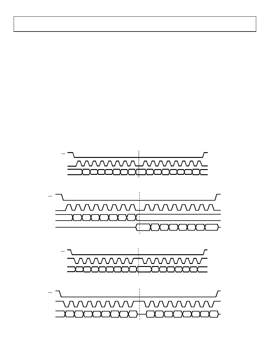
of SCLK. Figure 39 through Figure 42 are useful in understand-
ing the general operation of the AD9540 serial port.
.
04947-019
I6
I5
I4
I3
I2
I1
D5
D4
D3
D2
D1
D0
I0
D7
D6
I7
INSTRUCTION CYCLE
SCLK
SDI/O
DATA TRANSFER CYCLE
CS
Figure 39. Serial Port Write Timing—Clock Stall Low
04947-020
I6
I5
I4
I3
I2
I1
I0
DON'T CARE
I7
INSTRUCTION CYCLE
SCLK
SDI/O
DATA TRANSFER CYCLE
D5
D4
D3
D2
D1
D0
D7
D6
SDO
CS
Figure 40. 3-Wire Serial Port Read Timing—Clock Stall Low
04947-021
I6
I5
I4
I3
I2
I1
D5
D4
D3
D2
D1
D0
I0
D7
D6
I7
INSTRUCTION CYCLE
SCLK
SDI/O
DATA TRANSFER CYCLE
CS
Figure 41. Serial Port Write Timing—Clock Stall High
04947-022
I6
I5
I4
I3
I2
I1
D5
D4
D3
D2
D1
D0
I0
D7
D6
I7
INSTRUCTION CYCLE
SCLK
SDI/O
DATA TRANSFER CYCLE
CS
Figure 42. 2-Wire Serial Port Read Timing—Clock Stall High
相关PDF资料 |
PDF描述 |
|---|---|
| AD9547BCPZ-REEL7 | IC CLOCK GEN/SYNCHRONIZR 64LFCSP |
| AD9548BCPZ-REEL7 | IC CLOCK GEN/SYNCHRONIZR 88LFCSP |
| AD9549ABCPZ-REEL7 | IC CLOCK GEN/SYNCHRONIZR 64LFCSP |
| AD9550BCPZ-REEL7 | IC INTEGER-N TRANSLATOR 32-LFCSP |
| AD9551BCPZ | IC CLOCK GEN MULTISERV 40-LFCSP |
相关代理商/技术参数 |
参数描述 |
|---|---|
| AD9540PCB | 制造商:AD 制造商全称:Analog Devices 功能描述:655 MHz Low Jitter Clock Generator |
| AD9540-VCO/PCB | 制造商:Analog Devices 功能描述:EVAL BD FOR AD9540 ,655 MHZ LOW JITTER CLOCK GEN - Trays |
| AD9540-VCO/PCBZ | 功能描述:BOARD EVAL CLK GEN SYNTH 48LFCSP RoHS:是 类别:编程器,开发系统 >> 评估演示板和套件 系列:- 标准包装:1 系列:- 主要目的:电信,线路接口单元(LIU) 嵌入式:- 已用 IC / 零件:IDT82V2081 主要属性:T1/J1/E1 LIU 次要属性:- 已供物品:板,电源,线缆,CD 其它名称:82EBV2081 |
| AD9542/PCBZ | |
| AD9542BCPZ | 功能描述:SYNCHRONIZER & ADAPTIVE CLOCK TR 制造商:analog devices inc. 系列:* 包装:托盘 零件状态:在售 安装类型:表面贴装 封装/外壳:64-WFQFN 裸露焊盘 供应商器件封装:64-LFCSP(9x9) 标准包装:1 |
发布紧急采购,3分钟左右您将得到回复。