参数资料
| 型号: | AD9552BCPZ |
| 厂商: | Analog Devices Inc |
| 文件页数: | 17/32页 |
| 文件大小: | 0K |
| 描述: | IC PLL CLOCK GEN LP 32LFCSP |
| 设计资源: | Clock Distribution Circuit with Pin-Programmable Output Frequency, Output Logic Levels, and Fanout (CN0152) |
| 标准包装: | 1 |
| 类型: | 时钟发生器 |
| PLL: | 带旁路 |
| 输入: | CMOS,晶体 |
| 输出: | CMOS,LVDS,LVPECL |
| 电路数: | 1 |
| 比率 - 输入:输出: | 2:2 |
| 差分 - 输入:输出: | 无/是 |
| 频率 - 最大: | 900MHz |
| 除法器/乘法器: | 是/无 |
| 电源电压: | 3.135 V ~ 3.465 V |
| 工作温度: | -40°C ~ 85°C |
| 安装类型: | 表面贴装 |
| 封装/外壳: | 32-VFQFN 裸露焊盘,CSP |
| 供应商设备封装: | 32-LFCSP-VQ(5x5) |
| 包装: | 托盘 |
第1页第2页第3页第4页第5页第6页第7页第8页第9页第10页第11页第12页第13页第14页第15页第16页当前第17页第18页第19页第20页第21页第22页第23页第24页第25页第26页第27页第28页第29页第30页第31页第32页
AD9552
Data Sheet
Rev. E | Page 24 of 32
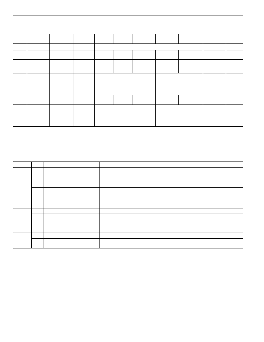
Addr.
(Hex)
Register
Name
(MSB) Bit 7
Bit 6
Bit 5
Bit 4
Bit 3
Bit 2
Bit 1
(LSB)
Bit 0
Default
capacitance
0x1C
XTAL
control
Unused
0x00
0x1D
XTAL
control
Unused
Select 2×
frequency
multiplier
Unused
Use crystal
resonator
0x00
0x32
OUT1
driver
control
OUT1 drive
strength
OUT1
power-
down
OUT1 mode control[2:0]
OUT1 CMOS polarity[1:0]
Enable SPI
control of
OUT1
driver
control
0xA8
0x33
Select OUT2
source
Unused
OUT2
source
Unused
0x00
0x34
OUT2
driver
control
OUT2 drive
strength
OUT2
power-
down
OUT2 mode control[2:0]
OUT2 CMOS polarity[1:0]
Enable SPI
control of
OUT2
driver
control
0xA8
REGISTER MAP DESCRIPTIONS
Control bit functions are active high unless stated otherwise. Register address values are always hexadecimal unless otherwise indicated.
Serial Port Control (Register 0x00 to Register 0x05)
Table 18.
Address
Bit
Bit Name
Description
0x00
7
Unused
Forced to Logic 0 internally, which enables 3-wire mode only.
6
LSB first
Bit order for SPI port.
0 = most significant bit and byte first (default).
1 = least significant bit and byte first.
5
Register map reset
Resets the register map to the default values. This is an autoclearing bit.
4
Unused
Forced to Logic 1 internally, which enables 16-bit mode (the only mode supported by
the device).
[3:0]
Unused
Mirrored version of the contents of Register 0x00[7:4] (that is, Bits[3:0] = Bits[7:4]).
0x04
[7:1]
Unused
Unused.
0
Readback control
For buffered registers, serial port readback reads from actual (active) registers instead of
from the buffer.
0 = reads values currently applied to the internal logic of the device (default).
1 = reads buffered values that take effect on next assertion of I/O update.
0x05
[7:1]
Unused
Unused.
0
I/O update
Writing a 1 to this bit transfers the data in the serial I/O buffer registers to the internal
control registers of the device. This is an autoclearing bit.
相关PDF资料 |
PDF描述 |
|---|---|
| VE-JVR-MZ-S | CONVERTER MOD DC/DC 7.5V 25W |
| ISL90841UIV1427Z | IC XDCP 256-TAP 50KOHM TSSOP-14 |
| SY100EP140LZG | IC FREQUENCY DETECTOR 3.3V 8SOIC |
| VE-JVP-MZ-S | CONVERTER MOD DC/DC 13.8V 25W |
| VI-B13-MY-F3 | CONVERTER MOD DC/DC 24V 50W |
相关代理商/技术参数 |
参数描述 |
|---|---|
| AD9552BCPZ | 制造商:Analog Devices 功能描述:IC PLL CLOCK GENERATOR 112.5MHZ LFCSP-32 |
| AD9552BCPZ-REEL7 | 功能描述:IC PLL CLOCK GEN LP 32LFCSP RoHS:是 类别:集成电路 (IC) >> 时钟/计时 - 时钟发生器,PLL,频率合成器 系列:- 标准包装:1,000 系列:Precision Edge® 类型:时钟/频率合成器 PLL:无 输入:CML,PECL 输出:CML 电路数:1 比率 - 输入:输出:2:1 差分 - 输入:输出:是/是 频率 - 最大:10.7GHz 除法器/乘法器:无/无 电源电压:2.375 V ~ 3.6 V 工作温度:-40°C ~ 85°C 安装类型:表面贴装 封装/外壳:16-VFQFN 裸露焊盘,16-MLF? 供应商设备封装:16-MLF?(3x3) 包装:带卷 (TR) 其它名称:SY58052UMGTRSY58052UMGTR-ND |
| AD9552PCBZ | 制造商:AD 制造商全称:Analog Devices 功能描述:Oscillator Frequency Upconverter |
| AD9553 | 制造商:AD 制造商全称:Analog Devices 功能描述:Flexible Clock Translator for GPON, Base Station, SONET/SDH, T1/E1, and Ethernet |
| AD9553/PCBZ | 功能描述:BOARD EVAL FOR AD9553 RoHS:是 类别:编程器,开发系统 >> 评估演示板和套件 系列:- 标准包装:1 系列:- 主要目的:电信,线路接口单元(LIU) 嵌入式:- 已用 IC / 零件:IDT82V2081 主要属性:T1/J1/E1 LIU 次要属性:- 已供物品:板,电源,线缆,CD 其它名称:82EBV2081 |
发布紧急采购,3分钟左右您将得到回复。