参数资料
| 型号: | AD9552BCPZ |
| 厂商: | Analog Devices Inc |
| 文件页数: | 23/32页 |
| 文件大小: | 0K |
| 描述: | IC PLL CLOCK GEN LP 32LFCSP |
| 设计资源: | Clock Distribution Circuit with Pin-Programmable Output Frequency, Output Logic Levels, and Fanout (CN0152) |
| 标准包装: | 1 |
| 类型: | 时钟发生器 |
| PLL: | 带旁路 |
| 输入: | CMOS,晶体 |
| 输出: | CMOS,LVDS,LVPECL |
| 电路数: | 1 |
| 比率 - 输入:输出: | 2:2 |
| 差分 - 输入:输出: | 无/是 |
| 频率 - 最大: | 900MHz |
| 除法器/乘法器: | 是/无 |
| 电源电压: | 3.135 V ~ 3.465 V |
| 工作温度: | -40°C ~ 85°C |
| 安装类型: | 表面贴装 |
| 封装/外壳: | 32-VFQFN 裸露焊盘,CSP |
| 供应商设备封装: | 32-LFCSP-VQ(5x5) |
| 包装: | 托盘 |
第1页第2页第3页第4页第5页第6页第7页第8页第9页第10页第11页第12页第13页第14页第15页第16页第17页第18页第19页第20页第21页第22页当前第23页第24页第25页第26页第27页第28页第29页第30页第31页第32页
Data Sheet
AD9552
Rev. E | Page 3 of 32
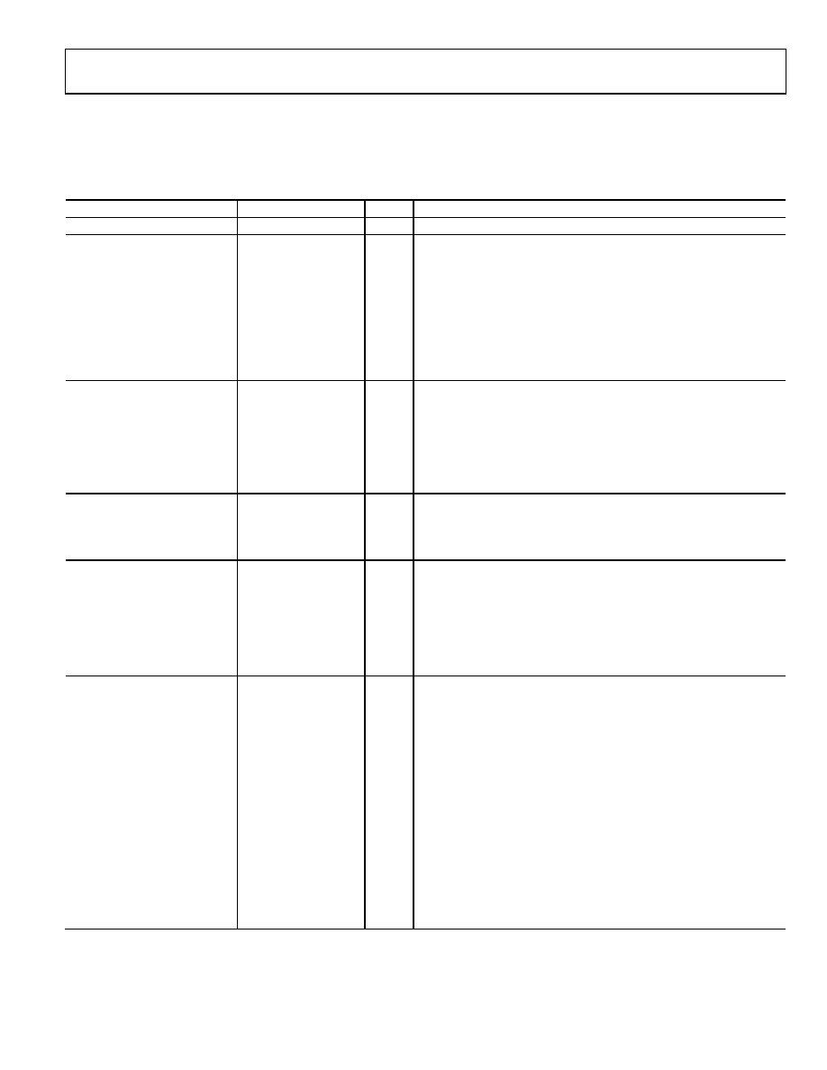
SPECIFICATIONS
Minimum (min) and maximum (max) values apply for the full range of supply voltage and operating temperature variations. Typical (typ)
values apply for VDD = 3.3 V; TA = 25°C, unless otherwise noted.
Table 1.
Parameter
Min
Typ
Max
Unit
Test Conditions/Comments
SUPPLY VOLTAGE
3.135
3.30
3.465
V
Pin 7, Pin 18, Pin 21, Pin 28
POWER CONSUMPTION
Total Current
149
169
mA
At maximum output frequency with both output channels active
VDD Current By Pin
Pin 7
2
3
mA
Pin 18
77
86
mA
Pin 21
35
41
mA
Pin 28
35
41
mA
LVPECL Output Driver
36
41
mA
900 MHz with 100 Ω termination between both pins of the output
driver
LOGIC INPUT PINS
INPUT CHARACTERISTICS1
Logic 1 Voltage, V
IH
1.0
V
For the CMOS inputs, a static Logic 1 results from either a pull-up
resistor or no connection
Logic 0 Voltage, V
IL
0.8
V
Logic 1 Current, I
IH
3
A
Logic 0 Current, I
IL
17
A
LOGIC OUTPUT PINS
Output Characteristics
Output Voltage High, V
OH
2.7
V
Output Voltage Low, V
OL
0.4
V
RESET PIN
Input Characteristics2
Input Voltage High, V
IH
1.8
V
Input Voltage Low, V
IL
1.3
V
Input Current High, I
INH
0.3
12.5
A
Input Current Low, I
INL
31
43
A
Minimum Pulse Width High
2
ns
REFERENCE CLOCK
INPUT CHARACTERISTICS
Frequency Range
7.94
MHz
N3 = 255; 2× frequency multiplier enabled; valid for all VCO bands
6.57
MHz
N3 = 255; 2× frequency multiplier enabled; f
VCO = 3.35 GHz, which con-
strains the frequency at OUT1 to be an integer sub-multiple of 3.35 GHz
(that is, f
OUT1 = 3.35 ÷ M GHz, where M is the product of the P0 and P1
output divider values)
93.06
MHz
71.28
MHz
SDM4 enabled; N3 = 476; valid for all VCO bands
112.5
MHz
VCO = 4.05 GHz, which constrains the
frequency at OUT1 to be an integer sub-multiple of 4.05 GHz (that is,
f
OUT1 = 4.05÷M GHz, where M is the product of the P0 and P1 output
divider values)
86.17
MHz
SDM4 enabled; N3 = 476; f
VCO = 4.05 GHz, which constrains the frequency
at OUT1 to be an integer sub-multiple of 4.05 GHz (that is, f
OUT1 =
4.05÷M GHz, where M is the product of the P
0 and P1 output divider
values)
相关PDF资料 |
PDF描述 |
|---|---|
| VE-JVR-MZ-S | CONVERTER MOD DC/DC 7.5V 25W |
| ISL90841UIV1427Z | IC XDCP 256-TAP 50KOHM TSSOP-14 |
| SY100EP140LZG | IC FREQUENCY DETECTOR 3.3V 8SOIC |
| VE-JVP-MZ-S | CONVERTER MOD DC/DC 13.8V 25W |
| VI-B13-MY-F3 | CONVERTER MOD DC/DC 24V 50W |
相关代理商/技术参数 |
参数描述 |
|---|---|
| AD9552BCPZ | 制造商:Analog Devices 功能描述:IC PLL CLOCK GENERATOR 112.5MHZ LFCSP-32 |
| AD9552BCPZ-REEL7 | 功能描述:IC PLL CLOCK GEN LP 32LFCSP RoHS:是 类别:集成电路 (IC) >> 时钟/计时 - 时钟发生器,PLL,频率合成器 系列:- 标准包装:1,000 系列:Precision Edge® 类型:时钟/频率合成器 PLL:无 输入:CML,PECL 输出:CML 电路数:1 比率 - 输入:输出:2:1 差分 - 输入:输出:是/是 频率 - 最大:10.7GHz 除法器/乘法器:无/无 电源电压:2.375 V ~ 3.6 V 工作温度:-40°C ~ 85°C 安装类型:表面贴装 封装/外壳:16-VFQFN 裸露焊盘,16-MLF? 供应商设备封装:16-MLF?(3x3) 包装:带卷 (TR) 其它名称:SY58052UMGTRSY58052UMGTR-ND |
| AD9552PCBZ | 制造商:AD 制造商全称:Analog Devices 功能描述:Oscillator Frequency Upconverter |
| AD9553 | 制造商:AD 制造商全称:Analog Devices 功能描述:Flexible Clock Translator for GPON, Base Station, SONET/SDH, T1/E1, and Ethernet |
| AD9553/PCBZ | 功能描述:BOARD EVAL FOR AD9553 RoHS:是 类别:编程器,开发系统 >> 评估演示板和套件 系列:- 标准包装:1 系列:- 主要目的:电信,线路接口单元(LIU) 嵌入式:- 已用 IC / 零件:IDT82V2081 主要属性:T1/J1/E1 LIU 次要属性:- 已供物品:板,电源,线缆,CD 其它名称:82EBV2081 |
发布紧急采购,3分钟左右您将得到回复。