- 您现在的位置:买卖IC网 > PDF目录16543 > AD9553/PCBZ (Analog Devices Inc)BOARD EVAL FOR AD9553 PDF资料下载
参数资料
| 型号: | AD9553/PCBZ |
| 厂商: | Analog Devices Inc |
| 文件页数: | 16/44页 |
| 文件大小: | 0K |
| 描述: | BOARD EVAL FOR AD9553 |
| 设计资源: | AD9553 Eval Brd BOM AD9553 Eval Brd Schematic |
| 标准包装: | 1 |
| 主要目的: | 计时,时钟缓冲器 / 驱动器 / 接收器 / 变换器 |
| 已用 IC / 零件: | AD9553 |
| 已供物品: | 板 |
| 相关产品: | AD9553BCPZ-ND - IC INTEGER-N CLCK GEN 32LFCSP AD9553BCPZ-REEL7-ND - IC INTEGER-N CLCK GEN 32LFCSP |
第1页第2页第3页第4页第5页第6页第7页第8页第9页第10页第11页第12页第13页第14页第15页当前第16页第17页第18页第19页第20页第21页第22页第23页第24页第25页第26页第27页第28页第29页第30页第31页第32页第33页第34页第35页第36页第37页第38页第39页第40页第41页第42页第43页第44页
AD9553
Rev. A | Page 23 of 44
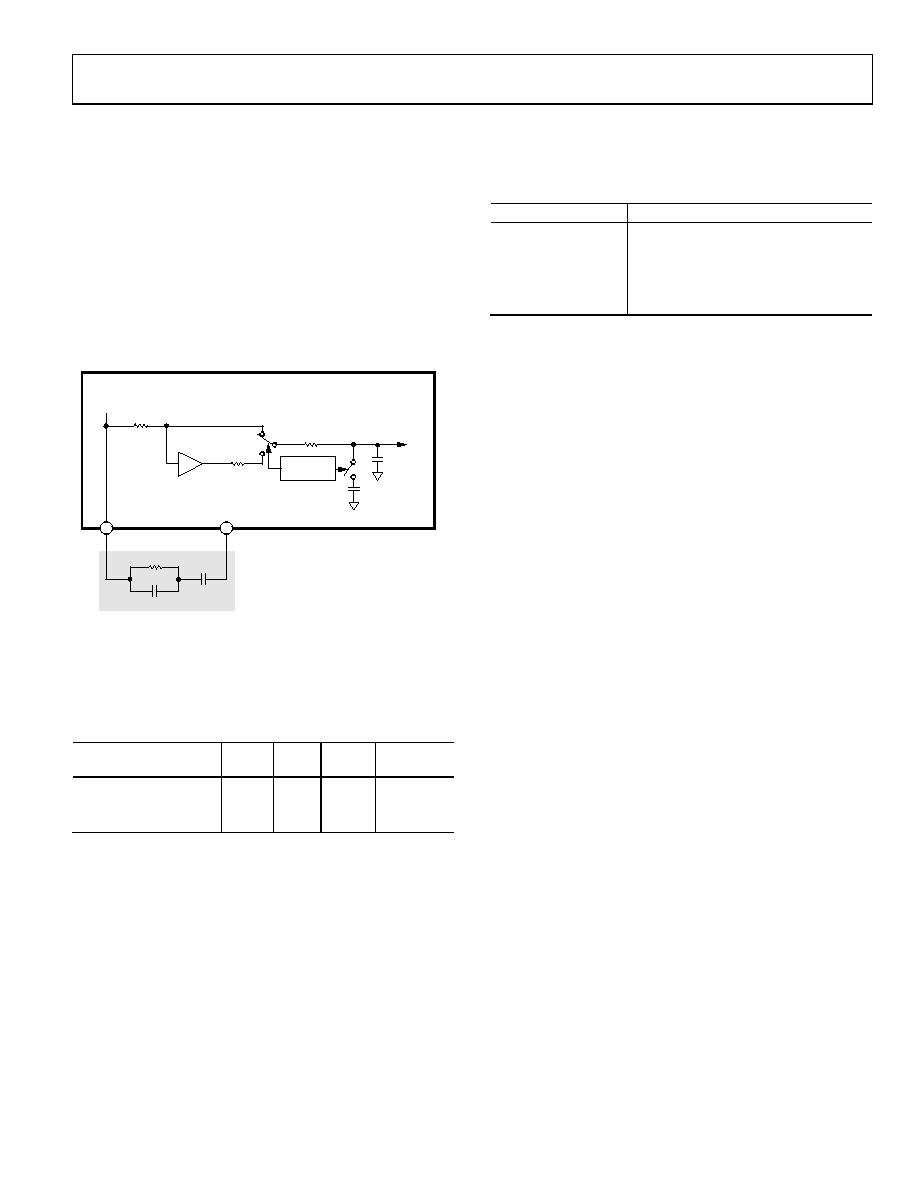
Loop Filter
The charge pump in the PFD delivers current to the loop filter
(see Figure 30). The components primarily responsible for the
bandwidth of the loop filter are external and connect between
Pin 16 and Pin 17.
The internal portion of the loop filter has two configurations: one
is for low loop bandwidth applications (~170 Hz) and the other is
for medium (~20 kHz)/high (~75 kHz) bandwidth applications.
The low loop bandwidth condition applies when the feedback
divider value (N) is 214 (16,384) or greater. Otherwise, the
medium/high loop bandwidth configuration is in effect. The
feedback divider value depends on the configuration of the Ax
and Yx pins per Table 16.
08565-
331
TO
VCO
3k
FILTER
53pF
C1
R
AD9553
C2
375
400k
BUFFER
170pF
CONTROL
LOGIC
SWITCHES CHANGE
STATE FOR N
≥ 16384
LDO
17
16
FROM
CHARGE
PUMP
Figure 30. External Loop Filter
The bandwidth of the loop filter primarily depends on three
external components (R, C1, and C2). There are two sets of recom-
mended values for these components corresponding to the low and
medium/high loop bandwidth configurations (see Table 17).
Table 17. External Loop Filter Components
A3 to A0 Pins
R
C1
C2
Loop
Bandwidth
0001 to 1100, and 1111
6.8 kΩ
47 nF
1 F
0.17 kHz
11101
12 kΩ
51 pF
220 nF
20 kHz
1101 and 11102
12 kΩ
51 pF
220 nF
75 kHz
1 The 20 kHz loop bandwidth case only applies when the A3 pin to A0 pin =
1110 and the Y5 pin to Y0 pin = 111111.
2 The 75 kHz loop bandwidth case only applies when the A3 pin to A0 pin =
1101 and the Y5 pin to Y0 pin = 101101 through 110010, or when the A3 pin
to A0 pin = 1110 and the Y5 pin to Y0 pin = 110011.
To achieve the best jitter performance in applications requiring a
loop bandwidth of less than 1 kHz, C1 and C2 must have an
insulation resistance of at least 500 F.
PLL Locked Indicator
The PLL provides a status indicator that appears at Pin 20
(LOCKED). When the PLL acquires phase lock, the LOCKED
pin switches to a Logic 1 state. When the PLL loses lock,
however, the LOCKED pin returns to a Logic 0 state.
Alternatively, the LOCKED pin serves as a test port allowing the
user to monitor one-of-four internal clocks. Register 0x17[3:1]
controls the test port as shown in Table 18.
Table 18. LOCKED Pin Output Control
Register 0x17[3:1]
LOCKED Pin Output
0XX
PLL locked indication (default)
100
Crystal oscillator clock signal
101
PFD pump-up clock divided-by-2
110
PFD reference input clock divided-by-2
111
PLL feedback to PFD clock divided-by-2
Output Dividers
The output divider section consists of three dividers: P0, P1, and P2.
The P0 divider (or VCO frequency prescaler) accepts the VCO
frequency and reduces it by a factor of 5 to 11 (selectable). This
brings the frequency down to a range between 305 MHz and
810 MHz.
The output of the P0 divider independently drives the P1 divider
and the P2 divider. The P1 divider establishes the frequency at
OUT1 and the P2 divider establishes the frequency at OUT2.
The P1 and P2 dividers are each programmable over a range of
1 to 1023, which results in a frequency at OUT1 or OUT2 that
is an integer submultiple of the frequency at the output of the P0
divider.
Output Driver Configuration
The user has complete control over all configurable parameters
of the OUT1 and OUT2 drivers via the OUT1 and OUT2 driver
control registers (Register 0x32 and Register 0x34, respectively,
as shown in Figure 31). To alter the parameters from their default
values, the user must use the SPI port to program the driver
control registers as desired.
The OUT1 and OUT2 drivers are configurable in terms of the
following parameters:
Logic family (via mode control)
Pin function (via mode control but only applies to the
CMOS family)
Polarity (only applies to the CMOS family)
Drive current
Power-down
Output Driver Mode Control
Three mode control bits establish the logic family and pin function
of the output drivers. The three bits originate either from Bits[5:3]
of Register 0x32 and Register 0x34 or from the decode logic
associated with the OM2 to OM0 pins as shown in Figure 31.
Note that Bit 0 of Register 0x32 and Register 0x34 determines
the source of the three mode control bits for the associated
output driver. Specifically, when Bit 0 of the register is Logic 0
(default), the source of the mode control bits for the associated
driver is the OM2 to OM0 pin decoder. When Bit 0 is Logic 1, the
source of the mode control bits is from Bits[5:3] of Register 0x32
and Register 0x34.
相关PDF资料 |
PDF描述 |
|---|---|
| ECE-T2WA561EA | CAP ALUM 560UF 450V 20% SNAP |
| 5503995-1 | CABLE ASSEM FIBER ST-ST 1 METER |
| M1BXK-2436J | IDC CABLE - MSR24K/MC24G/X |
| 5504970-5 | CABLE ASSEM FIBER SC-SC 10METER |
| AD812AR-EBZ | BOARD EVAL FOR AD812AR |
相关代理商/技术参数 |
参数描述 |
|---|---|
| AD9554/PCBZ | 功能描述:AD9554 - Timing, Clock Generator Evaluation Board 制造商:analog devices inc. 系列:- 零件状态:有效 主要用途:计时,时钟发生器 嵌入式:- 使用的 IC/零件:AD9554 主要属性:- 辅助属性:LED 状态指示器 所含物品:板 标准包装:1 |
| AD9554-1/PCBZ | 功能描述:AD9554-1 - Timing, Clock Generator Evaluation Board 制造商:analog devices inc. 系列:- 零件状态:有效 主要用途:计时,时钟发生器 嵌入式:- 使用的 IC/零件:AD9554-1 主要属性:- 辅助属性:LED 状态指示器 所含物品:板 标准包装:1 |
| AD9554-1BCPZ | 功能描述:IC PLL CLOCK GEN 4OUT 72LFCSP 制造商:analog devices inc. 系列:- 包装:托盘 零件状态:有效 PLL:是 主要用途:以太网,SONET/SDH,Stratum 输入:CMOS,LVDS 输出:HCSL,LVDS,LVPECL 电路数:1 比率 - 输入:输出:4:4 差分 - 输入:输出:是/是 频率 - 最大值:942MHz 电压 - 电源:1.4 V ~ 2.625 V 工作温度:-40°C ~ 85°C 安装类型:表面贴装 封装/外壳:56-WFQFN 裸焊盘,CSP 供应商器件封装:56-LFCSP-WQ(8x8) 标准包装:1 |
| AD9554-1BCPZ-REEL7 | 功能描述:IC PLL CLOCK GEN 4OUT 72LFCSP 制造商:analog devices inc. 系列:- 包装:带卷(TR) 零件状态:有效 PLL:是 主要用途:以太网,SONET/SDH,Stratum 输入:CMOS,LVDS 输出:HCSL,LVDS,LVPECL 电路数:1 比率 - 输入:输出:4:4 差分 - 输入:输出:是/是 频率 - 最大值:942MHz 电压 - 电源:1.4 V ~ 2.625 V 工作温度:-40°C ~ 85°C 安装类型:表面贴装 封装/外壳:56-WFQFN 裸焊盘,CSP 供应商器件封装:56-LFCSP-WQ(8x8) 标准包装:750 |
| AD9554BCPZ | 功能描述:IC CLOCK TRANSLATOR 8OUT 72LFCSP 制造商:analog devices inc. 系列:- 包装:托盘 零件状态:有效 PLL:是 主要用途:以太网,SONET/SDH,Stratum 输入:CMOS,LVDS 输出:HCSL,LVDS,LVPECL 电路数:1 比率 - 输入:输出:4:8 差分 - 输入:输出:是/是 频率 - 最大值:941MHz 电压 - 电源:1.47 V ~ 1.89 V 工作温度:-40°C ~ 85°C 安装类型:表面贴装 封装/外壳:72-VFQFN 裸露焊盘,CSP 供应商器件封装:72-LFCSP-VQ(10x10) 标准包装:1 |
发布紧急采购,3分钟左右您将得到回复。