- 您现在的位置:买卖IC网 > PDF目录16543 > AD9553/PCBZ (Analog Devices Inc)BOARD EVAL FOR AD9553 PDF资料下载
参数资料
| 型号: | AD9553/PCBZ |
| 厂商: | Analog Devices Inc |
| 文件页数: | 25/44页 |
| 文件大小: | 0K |
| 描述: | BOARD EVAL FOR AD9553 |
| 设计资源: | AD9553 Eval Brd BOM AD9553 Eval Brd Schematic |
| 标准包装: | 1 |
| 主要目的: | 计时,时钟缓冲器 / 驱动器 / 接收器 / 变换器 |
| 已用 IC / 零件: | AD9553 |
| 已供物品: | 板 |
| 相关产品: | AD9553BCPZ-ND - IC INTEGER-N CLCK GEN 32LFCSP AD9553BCPZ-REEL7-ND - IC INTEGER-N CLCK GEN 32LFCSP |
第1页第2页第3页第4页第5页第6页第7页第8页第9页第10页第11页第12页第13页第14页第15页第16页第17页第18页第19页第20页第21页第22页第23页第24页当前第25页第26页第27页第28页第29页第30页第31页第32页第33页第34页第35页第36页第37页第38页第39页第40页第41页第42页第43页第44页
AD9553
Rev. A | Page 31 of 44
By default, a read request reads the register value that is currently
in use by the AD9553. However, setting Register 0x04[0] = 1
causes the buffered registers to be read instead. The buffered
registers are the ones that take effect during the next I/O update.
AD9553
CORE
C
ON
TR
OL
R
E
GIS
TE
R
S
SERIAL
CONTROL
PORT
RE
G
IS
T
E
R
BUF
F
E
RS
13
14
12
OM1/SCLK
OM0/SDIO
OM2/CS
EXECUTE AN
INPUT/OUTPUT
UPDATE
REGISTER
UPDATE
08565-
007
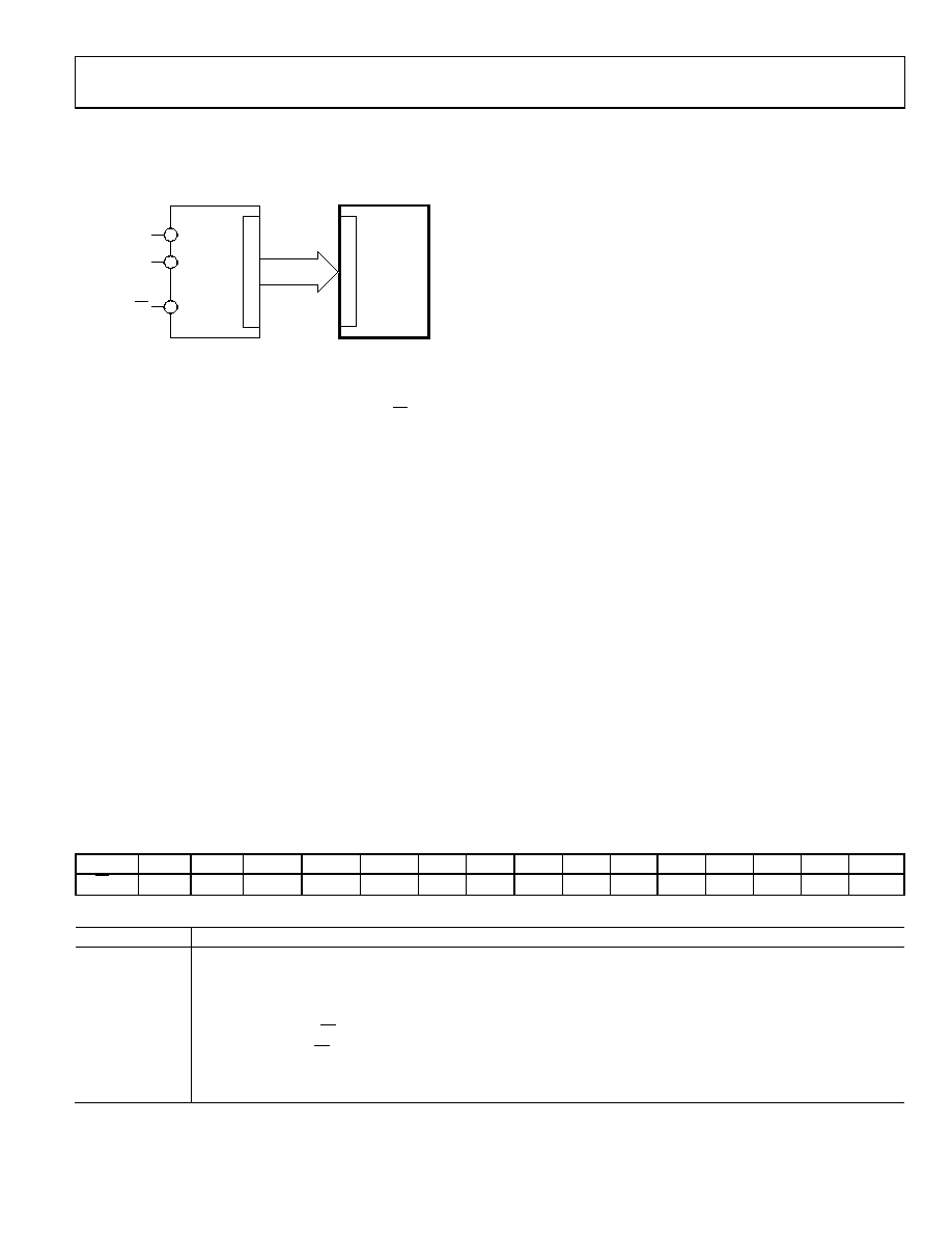
Figure 35. Relationship Between the Serial Control Port Register Buffers
and the Control Registers
INSTRUCTION WORD (16 BITS)
indicates whether the instruction is a read or a write. The next
two bits, W1 and W0, are the transfer length in bytes. The final
13 bits are the address bits (Address Bits[A12:A0]) at which the
read or write operation is to begin.
For a write, the instruction word is followed by the number of
bytes of data indicated by Bits[W1:W0], which is interpreted
according to Table 24.
Address Bits[A12:A0] select the address within the register map
that is written to or read from during the data transfer portion
of the communication cycle. The AD9553 uses all of the 13-bit
address space. For multibyte transfers, this address is the starting
byte address.
MSB/LSB FIRST TRANSFERS
The AD9553 instruction word and byte data can be MSB first or
LSB first. The default for the AD9553 is MSB first. The LSB first
mode can be set by writing a 1 to Register 0x00[6] and requires
that an I/O update be executed. Immediately after the LSB first
bit is set, all serial control port operations are changed to LSB
first order.
When MSB first mode is active, the instruction and data bytes
must be written from MSB to LSB. Multibyte data transfers in
MSB first format start with an instruction byte that includes the
register address of the most significant data byte. Subsequent
data bytes must follow in order from high address to low address.
In MSB first mode, the serial control port internal address gen-
erator decrements for each data byte of the multibyte transfer cycle.
When LSB first = 1 (LSB first), the instruction and data bytes
must be written from LSB to MSB. Multibyte data transfers
in LSB first format start with an instruction byte that includes
the register address of the least significant data byte followed
by multiple data bytes. The serial control port internal byte
address generator increments for each data byte of the multibyte
transfer cycle.
The AD9553 serial control port register address decrements from
the register address just written toward 0x00 for multibyte I/O
operations if the MSB first mode is active (default). If the LSB
first mode is active, the serial control port register address
increments from the address just written toward 0x34 for
multibyte I/O operations.
Unused addresses are not skipped during multibyte I/O operations.
The user should write the default value to a reserved register and
should write only zeros to unmapped registers. Note that it is more
efficient to issue a new write command than to write the default
value to more than two consecutive reserved (or unmapped)
registers.
Table 25. Serial Control Port, 16-Bit Instruction Word, MSB First
MSB
LSB
I15
I14
I13
I12
I11
I10
I9
I8
I7
I6
I5
I4
I3
I2
I1
I0
R/W
W1
W0
A12
A11
A10
A9
A8
A7
A6
A5
A4
A3
A2
A1
A0
Table 26. Definition of Terms Used in Serial Control Port Timing Diagrams
Parameter
Description
t
CLK
Period of SCLK
t
DV
Read data valid time (time from falling edge of SCLK to valid data on SDIO)
t
DS
Setup time between data and rising edge of SCLK
t
DH
Hold time between data and rising edge of SCLK
t
S
Setup time between CS and SCLK
t
H
Hold time between CS and SCLK
t
HIGH
Minimum period that SCLK should be in a logic high state
t
LOW
Minimum period that SCLK should be in a logic low state
相关PDF资料 |
PDF描述 |
|---|---|
| ECE-T2WA561EA | CAP ALUM 560UF 450V 20% SNAP |
| 5503995-1 | CABLE ASSEM FIBER ST-ST 1 METER |
| M1BXK-2436J | IDC CABLE - MSR24K/MC24G/X |
| 5504970-5 | CABLE ASSEM FIBER SC-SC 10METER |
| AD812AR-EBZ | BOARD EVAL FOR AD812AR |
相关代理商/技术参数 |
参数描述 |
|---|---|
| AD9554/PCBZ | 功能描述:AD9554 - Timing, Clock Generator Evaluation Board 制造商:analog devices inc. 系列:- 零件状态:有效 主要用途:计时,时钟发生器 嵌入式:- 使用的 IC/零件:AD9554 主要属性:- 辅助属性:LED 状态指示器 所含物品:板 标准包装:1 |
| AD9554-1/PCBZ | 功能描述:AD9554-1 - Timing, Clock Generator Evaluation Board 制造商:analog devices inc. 系列:- 零件状态:有效 主要用途:计时,时钟发生器 嵌入式:- 使用的 IC/零件:AD9554-1 主要属性:- 辅助属性:LED 状态指示器 所含物品:板 标准包装:1 |
| AD9554-1BCPZ | 功能描述:IC PLL CLOCK GEN 4OUT 72LFCSP 制造商:analog devices inc. 系列:- 包装:托盘 零件状态:有效 PLL:是 主要用途:以太网,SONET/SDH,Stratum 输入:CMOS,LVDS 输出:HCSL,LVDS,LVPECL 电路数:1 比率 - 输入:输出:4:4 差分 - 输入:输出:是/是 频率 - 最大值:942MHz 电压 - 电源:1.4 V ~ 2.625 V 工作温度:-40°C ~ 85°C 安装类型:表面贴装 封装/外壳:56-WFQFN 裸焊盘,CSP 供应商器件封装:56-LFCSP-WQ(8x8) 标准包装:1 |
| AD9554-1BCPZ-REEL7 | 功能描述:IC PLL CLOCK GEN 4OUT 72LFCSP 制造商:analog devices inc. 系列:- 包装:带卷(TR) 零件状态:有效 PLL:是 主要用途:以太网,SONET/SDH,Stratum 输入:CMOS,LVDS 输出:HCSL,LVDS,LVPECL 电路数:1 比率 - 输入:输出:4:4 差分 - 输入:输出:是/是 频率 - 最大值:942MHz 电压 - 电源:1.4 V ~ 2.625 V 工作温度:-40°C ~ 85°C 安装类型:表面贴装 封装/外壳:56-WFQFN 裸焊盘,CSP 供应商器件封装:56-LFCSP-WQ(8x8) 标准包装:750 |
| AD9554BCPZ | 功能描述:IC CLOCK TRANSLATOR 8OUT 72LFCSP 制造商:analog devices inc. 系列:- 包装:托盘 零件状态:有效 PLL:是 主要用途:以太网,SONET/SDH,Stratum 输入:CMOS,LVDS 输出:HCSL,LVDS,LVPECL 电路数:1 比率 - 输入:输出:4:8 差分 - 输入:输出:是/是 频率 - 最大值:941MHz 电压 - 电源:1.47 V ~ 1.89 V 工作温度:-40°C ~ 85°C 安装类型:表面贴装 封装/外壳:72-VFQFN 裸露焊盘,CSP 供应商器件封装:72-LFCSP-VQ(10x10) 标准包装:1 |
发布紧急采购,3分钟左右您将得到回复。