- 您现在的位置:买卖IC网 > PDF目录1987 > AD9553BCPZ-REEL7 (Analog Devices Inc)IC INTEGER-N CLCK GEN 32LFCSP PDF资料下载
参数资料
| 型号: | AD9553BCPZ-REEL7 |
| 厂商: | Analog Devices Inc |
| 文件页数: | 19/44页 |
| 文件大小: | 0K |
| 描述: | IC INTEGER-N CLCK GEN 32LFCSP |
| 标准包装: | 1,500 |
| 类型: | 时钟/频率转换器 |
| PLL: | 是 |
| 主要目的: | 以太网,GPON,SONET/SHD,T1/E1 |
| 输入: | CMOS,LVDS,晶体 |
| 输出: | CMOS,LVDS,LVPECL |
| 电路数: | 1 |
| 比率 - 输入:输出: | 1:2 |
| 差分 - 输入:输出: | 是/是 |
| 频率 - 最大: | 810MHz |
| 电源电压: | 3.135 V ~ 3.465 V |
| 工作温度: | -40°C ~ 85°C |
| 安装类型: | 表面贴装 |
| 封装/外壳: | 32-WFQFN 裸露焊盘,CSP |
| 供应商设备封装: | 32-LFCSP(5x5) |
| 包装: | 带卷 (TR) |
| 配用: | AD9553/PCBZ-ND - BOARD EVAL FOR AD9553 |
第1页第2页第3页第4页第5页第6页第7页第8页第9页第10页第11页第12页第13页第14页第15页第16页第17页第18页当前第19页第20页第21页第22页第23页第24页第25页第26页第27页第28页第29页第30页第31页第32页第33页第34页第35页第36页第37页第38页第39页第40页第41页第42页第43页第44页
AD9553
Rev. A | Page 26 of 44
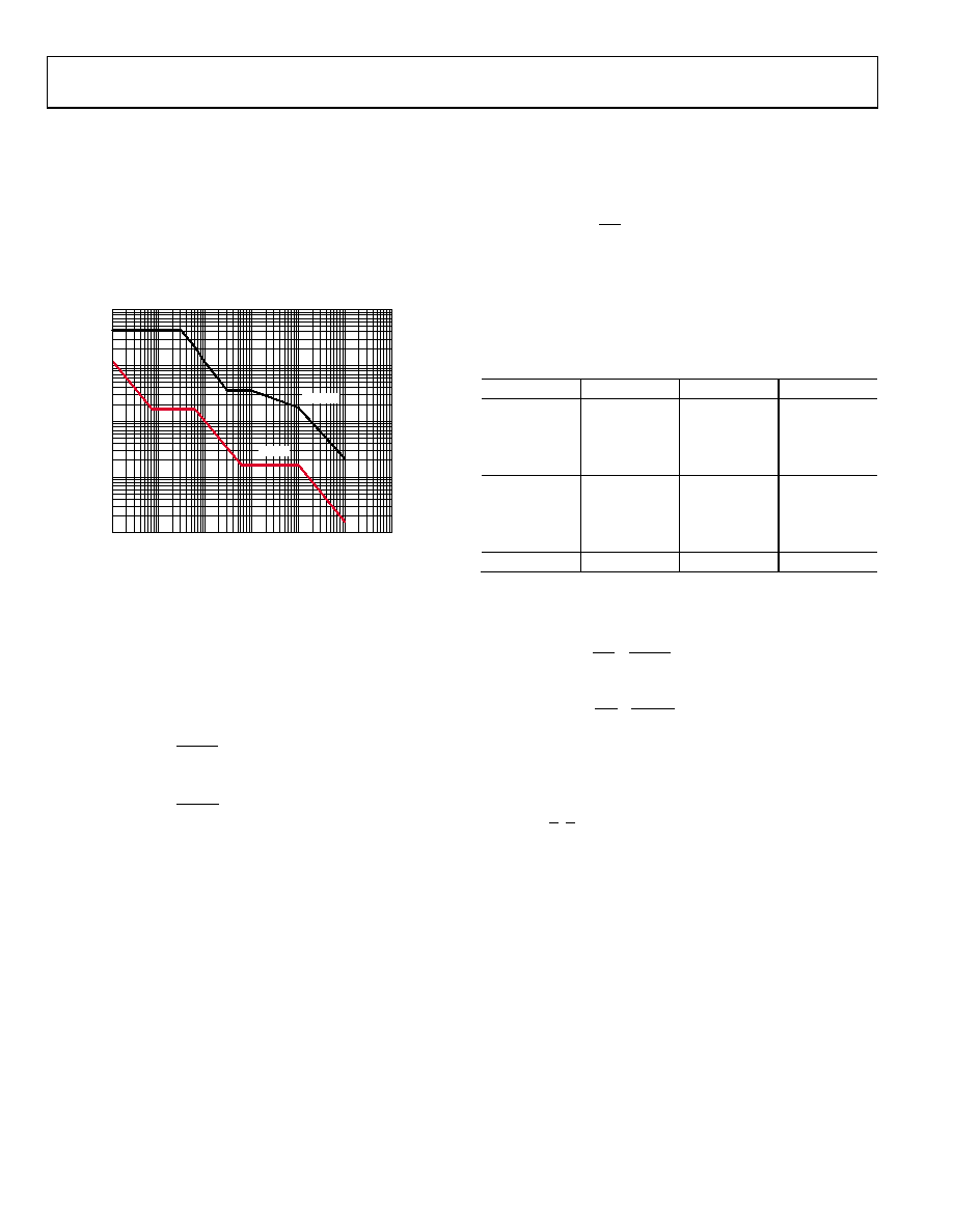
JITTER TOLERANCE
Jitter tolerance is the ability of the AD9553 to maintain lock in
the presence of sinusoidal jitter. The AD9553 meets the input
jitter tolerance mask per Telcordia GR-253-CORE (see Figure 32).
The acceptable jitter tolerance is the region above the mask. The
trace showing the performance of the AD9553 in Figure 32
represents the limitations of the test equipment because the
AD9553 did not indicate loss of lock, even with the test
equipment injecting its maximum jitter level.
1k
0.1
1
10
100
0.01
0.1
1
10
100
1k
10k
IN
P
U
T
J
ITTE
R
A
M
P
LITU
D
E
(
U
L
PP
)
JITTER FREQUENCY (kHz)
08565-
030
AD9553
MASK
Figure 32. Jitter Tolerance
OUTPUT/INPUT FREQUENCY RELATIONSHIP
The frequency at OUT1 and OUT2 depends on the frequency at
the input to the PLL, the PLL feedback divider value (N), and the
output divider values (P0, P1, and P2). The equations that define
the frequency at OUT1 and OUT2 (fOUT1 and fOUT2, respectively)
are as follows:
×
=
1
0
1
P
N
FPFD
fOUT
×
=
2
0
2
P
N
FPFD
fOUT
where:
FPFD is the frequency at the reference input of the PFD.
N is the feedback divider value.
P0 is the VCO prescaler divider value.
P1 is the OUT1 divider value.
P2 is the OUT2 divider value.
The operating frequency range of the PFD places a limitation
on FPFD as follows:
13.3 kHz ≤ FPFD ≤ 100 MHz
Note that for applications using the frequency selection pins in
conjunction with the XTAL input for the holdover function, the
maximum value of FPFD is 50 MHz (twice the 25 MHz default
crystal frequency).
FPFD depends on the input frequency to the AD9553, the
configuration of the multiplexers for the ÷5 prescaler and ×2
frequency multiplier, and the value of the RX divider (either RA,
RB, or RXO) as follows:
X
R
K
f
FPFD
×
=
where:
fX is equal to fREFA, fREFB, or fXTAL.
K is the scale factor per Table 22.
FPFD is the frequency at the input to the phase frequency
detector.
Table 22. K as a Function of Input Multiplexer Configuration
Input
÷5
×2
K
REFA
Bypassed
1
Active
Bypassed
1/5
Bypassed
Active
2
Active
2/5
REFB
Bypassed
1
Active
Bypassed
1/5
Bypassed
Active
2
Active
2/5
XTAL
2
1 N/A means not applicable.
This leads to the complete frequency translation formula
×
=
1
0
1
P
N
R
K
f
X
OUT
×
=
2
0
2
P
N
R
K
f
X
OUT
Specific numeric constraints apply as follows. Note that the
symbol ∈ indicates that the constraint is an element of one in
the series from the list within the curly brackets.
K
∈
2
,1
,
5
2
,
5
1
KX∈ {1, 2, …, 16,384}
N∈ {32, 33, …, 1,048,576}
P0∈ {5, 6, …, 11}
P1∈ {1, 2, …, 63}
P2∈ {1, 2, …, 63}
Additional constraints apply. One constraint is related to the
VCO and the other to the ×2 frequency multipliers in the REFA
and REFB paths. The VCO constraint is a consequence of its
limited bandwidth. However, the ×2 frequency multiplier
constraint only applies when the ÷5 prescalers are bypassed, but
it also requires that RA and RB are large enough to satisfy the
FPFD constraint. The additional constraints are as follows:
3350 MHz ≤ fOUT1 × P0 × P1 ≤ 4050 MHz
3350 MHz ≤ fOUT2 × P0 × P2 ≤ 4050 MHz
fREFA/REFB ≤ 125 MHz (×2 multiplier with ÷5 bypassed)
相关PDF资料 |
PDF描述 |
|---|---|
| AD9557BCPZ-REEL7 | IC CLK XLATR PLL 1250MHZ 40LFCSP |
| AD9558BCPZ-REEL7 | IC CLK XLATR PLL 1250MHZ 64LFCSP |
| AD9571ACPZPEC-R7 | IC PLL CLOCK GEN 25MHZ 40LFCSP |
| AD9572ACPZLVD-R7 | IC PLL CLOCK GEN 25MHZ 40LFCSP |
| AD9573ARUZ-RL7 | IC PCI CLCOK GEN 25MHZ 16TSSOP |
相关代理商/技术参数 |
参数描述 |
|---|---|
| AD9554/PCBZ | 功能描述:AD9554 - Timing, Clock Generator Evaluation Board 制造商:analog devices inc. 系列:- 零件状态:有效 主要用途:计时,时钟发生器 嵌入式:- 使用的 IC/零件:AD9554 主要属性:- 辅助属性:LED 状态指示器 所含物品:板 标准包装:1 |
| AD9554-1/PCBZ | 功能描述:AD9554-1 - Timing, Clock Generator Evaluation Board 制造商:analog devices inc. 系列:- 零件状态:有效 主要用途:计时,时钟发生器 嵌入式:- 使用的 IC/零件:AD9554-1 主要属性:- 辅助属性:LED 状态指示器 所含物品:板 标准包装:1 |
| AD9554-1BCPZ | 功能描述:IC PLL CLOCK GEN 4OUT 72LFCSP 制造商:analog devices inc. 系列:- 包装:托盘 零件状态:有效 PLL:是 主要用途:以太网,SONET/SDH,Stratum 输入:CMOS,LVDS 输出:HCSL,LVDS,LVPECL 电路数:1 比率 - 输入:输出:4:4 差分 - 输入:输出:是/是 频率 - 最大值:942MHz 电压 - 电源:1.4 V ~ 2.625 V 工作温度:-40°C ~ 85°C 安装类型:表面贴装 封装/外壳:56-WFQFN 裸焊盘,CSP 供应商器件封装:56-LFCSP-WQ(8x8) 标准包装:1 |
| AD9554-1BCPZ-REEL7 | 功能描述:IC PLL CLOCK GEN 4OUT 72LFCSP 制造商:analog devices inc. 系列:- 包装:带卷(TR) 零件状态:有效 PLL:是 主要用途:以太网,SONET/SDH,Stratum 输入:CMOS,LVDS 输出:HCSL,LVDS,LVPECL 电路数:1 比率 - 输入:输出:4:4 差分 - 输入:输出:是/是 频率 - 最大值:942MHz 电压 - 电源:1.4 V ~ 2.625 V 工作温度:-40°C ~ 85°C 安装类型:表面贴装 封装/外壳:56-WFQFN 裸焊盘,CSP 供应商器件封装:56-LFCSP-WQ(8x8) 标准包装:750 |
| AD9554BCPZ | 功能描述:IC CLOCK TRANSLATOR 8OUT 72LFCSP 制造商:analog devices inc. 系列:- 包装:托盘 零件状态:有效 PLL:是 主要用途:以太网,SONET/SDH,Stratum 输入:CMOS,LVDS 输出:HCSL,LVDS,LVPECL 电路数:1 比率 - 输入:输出:4:8 差分 - 输入:输出:是/是 频率 - 最大值:941MHz 电压 - 电源:1.47 V ~ 1.89 V 工作温度:-40°C ~ 85°C 安装类型:表面贴装 封装/外壳:72-VFQFN 裸露焊盘,CSP 供应商器件封装:72-LFCSP-VQ(10x10) 标准包装:1 |
发布紧急采购,3分钟左右您将得到回复。