- 您现在的位置:买卖IC网 > PDF目录1987 > AD9553BCPZ-REEL7 (Analog Devices Inc)IC INTEGER-N CLCK GEN 32LFCSP PDF资料下载
参数资料
| 型号: | AD9553BCPZ-REEL7 |
| 厂商: | Analog Devices Inc |
| 文件页数: | 8/44页 |
| 文件大小: | 0K |
| 描述: | IC INTEGER-N CLCK GEN 32LFCSP |
| 标准包装: | 1,500 |
| 类型: | 时钟/频率转换器 |
| PLL: | 是 |
| 主要目的: | 以太网,GPON,SONET/SHD,T1/E1 |
| 输入: | CMOS,LVDS,晶体 |
| 输出: | CMOS,LVDS,LVPECL |
| 电路数: | 1 |
| 比率 - 输入:输出: | 1:2 |
| 差分 - 输入:输出: | 是/是 |
| 频率 - 最大: | 810MHz |
| 电源电压: | 3.135 V ~ 3.465 V |
| 工作温度: | -40°C ~ 85°C |
| 安装类型: | 表面贴装 |
| 封装/外壳: | 32-WFQFN 裸露焊盘,CSP |
| 供应商设备封装: | 32-LFCSP(5x5) |
| 包装: | 带卷 (TR) |
| 配用: | AD9553/PCBZ-ND - BOARD EVAL FOR AD9553 |
第1页第2页第3页第4页第5页第6页第7页当前第8页第9页第10页第11页第12页第13页第14页第15页第16页第17页第18页第19页第20页第21页第22页第23页第24页第25页第26页第27页第28页第29页第30页第31页第32页第33页第34页第35页第36页第37页第38页第39页第40页第41页第42页第43页第44页
AD9553
Rev. A | Page 16 of 44
THEORY OF OPERATION
A[3:0]
REGISTER BANK
OUTPUT MODE/
SERIAL PORT
PRECONFIGURED
DIVIDER SETTINGS
REFA
XTAL
Y[5:0]
4
6
3
XTAL
VCO
AD9553
OUT1
3350MHz
TO
4050MHz
LOCKED
FILTER
2
N
P
F
D
OUT2
2
20
3
10
P0
P1
P2
P0
P1
DN
UP
3
SPI CTRL
3
×2
FDBK
REFERENCE
SWITCHOVER
CONTROL
CLOCK
MUX
CLOCK MUX
HOLD
REF
SEL
DET
A
DET
B
DET
XO
SEL REFB
DCXO
CTRL
TEST
1 0
0
1
0
1
0
1
RA, ×2A, ÷5A
RB, ×2B, ÷5B
RXO, DCXO CTRL
N, P0, P1, P2
REF SEL
TEST
REF DIFF
REF
DIFF
÷5
0
1
÷5A
÷5
0
1
÷5B
REFB/REFA
XO
FPFD
PLL
14
DET
DET A
0
1
÷RA
÷N
×2A
RA
×2
14
DET
DET B
0
1
÷RB
×2B
RB
×2
14
DET
DET XO
÷RXO
RXO
TUNING
CONTROL
UP/2
FPFD/2
FDBK/2
XO
LOCK
DETECT
OUTPUT
MODE
CONTROL
5 TO 11
LOOP
FILTER
CHARGE
PUMP
08565-
101
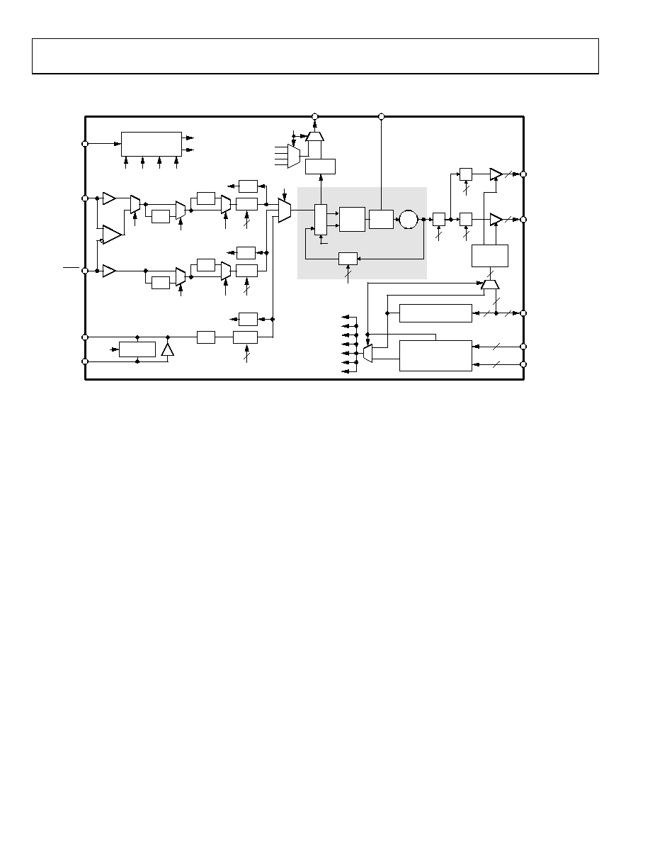
Figure 27. Detailed Block Diagram
OVERVIEW
The AD9553 can receive up to two input reference clocks, REFA
and REFB. Both input clock paths include an optional divide-by-5
(÷5) prescaler, an optional ×2 frequency multiplier, and a 14-bit
programmable divider. Alternatively, the user can program the
device to operate with one differential input clock (instead of
two single-ended input clocks) via the serial I/O port. In the
differential operating mode, the REFB path is inactive.
The AD9553 also has a dedicated XTAL input for direct connec-
tion of an optional 25 MHz crystal resonator. This allows for a
backup clock signal useful for holdover operation in case both
input references fail. The XTAL clock path includes a fixed ×2
frequency multiplier and a 14-bit programmable divider.
The AD9553 includes a switchover control block that auto-
matically handles switching from REFA to REFB (or vice versa)
in the event of a reference failure. If both REFA and REFB fail,
however, then the switchover control block automatically enters
holdover mode by selecting the XTAL clock signal (assuming
the presence of a crystal resonator at the XTAL input).
Generally, the clock signals that appear at the input to the clock
multiplexer (see Figure 27) all operate at the same frequency.
Thus, the frequency at the input to the PLL (FPFD in Figure 27)
is the same regardless of the signal selected by the clock multi-
plexer. The PLL converts FPFD to a frequency within the operating
range of the VCO (3.35 GHz to 4.05 GHz) based on the value of
the feedback divider (N). The VCO prescaler (P0) reduces the
VCO output frequency by an integer factor of 5 to 11, resulting in
an intermediate frequency in the range of 305 MHz to 810 MHz.
The 10-bit P1 and P2 dividers can further reduce the P0 output
frequency to yield the final output clock frequencies at OUT1
and OUT2, respectively.
Thus, the frequency translation ratio from the reference input
to the output depends on the selection of the ÷5 prescalers; the
×2 frequency multipliers; the values of the three R dividers; the
N divider; and the P0, P1, and P2 dividers. These parameters are
set automatically via the preconfigured divider settings per the Ax
and Yx pins (see the Preset Frequencies section). Alternatively, the
user can custom program these parameters via the serial I/O port
(see the Serial Control Port and Register Map sections), which allows
the device to accommodate custom frequency translation ratios.
PRESET FREQUENCIES
The frequency selection pins (A3 to A0 and Y5 to Y0) allow the
user to hardwire the device for preset input and output frequencies
based on the pin logic states (see Figure 27). The pins decode
ground or open connections as Logic 0 or Logic 1, respectively.
To have access to the device control registers via the SPI port, the
user must select Pin Y5 to Pin Y0 = 000000 and/or Pin A3 to
Pin A0 = 0000. Doing so causes Pin 12 through Pin 14 to function
as SPI port control pins instead of output mode control pins (see
the Output Driver Mode Control section). Note that after selecting
SPI mode, the user must write a Logic 1 to Bit 0 of Register 0x32
and Register 0x34 to enable the registers as the source of the OUT1
and OUT2 mode control bits (see Figure 31 and the Output Driver
Mode Control section).
相关PDF资料 |
PDF描述 |
|---|---|
| AD9557BCPZ-REEL7 | IC CLK XLATR PLL 1250MHZ 40LFCSP |
| AD9558BCPZ-REEL7 | IC CLK XLATR PLL 1250MHZ 64LFCSP |
| AD9571ACPZPEC-R7 | IC PLL CLOCK GEN 25MHZ 40LFCSP |
| AD9572ACPZLVD-R7 | IC PLL CLOCK GEN 25MHZ 40LFCSP |
| AD9573ARUZ-RL7 | IC PCI CLCOK GEN 25MHZ 16TSSOP |
相关代理商/技术参数 |
参数描述 |
|---|---|
| AD9554/PCBZ | 功能描述:AD9554 - Timing, Clock Generator Evaluation Board 制造商:analog devices inc. 系列:- 零件状态:有效 主要用途:计时,时钟发生器 嵌入式:- 使用的 IC/零件:AD9554 主要属性:- 辅助属性:LED 状态指示器 所含物品:板 标准包装:1 |
| AD9554-1/PCBZ | 功能描述:AD9554-1 - Timing, Clock Generator Evaluation Board 制造商:analog devices inc. 系列:- 零件状态:有效 主要用途:计时,时钟发生器 嵌入式:- 使用的 IC/零件:AD9554-1 主要属性:- 辅助属性:LED 状态指示器 所含物品:板 标准包装:1 |
| AD9554-1BCPZ | 功能描述:IC PLL CLOCK GEN 4OUT 72LFCSP 制造商:analog devices inc. 系列:- 包装:托盘 零件状态:有效 PLL:是 主要用途:以太网,SONET/SDH,Stratum 输入:CMOS,LVDS 输出:HCSL,LVDS,LVPECL 电路数:1 比率 - 输入:输出:4:4 差分 - 输入:输出:是/是 频率 - 最大值:942MHz 电压 - 电源:1.4 V ~ 2.625 V 工作温度:-40°C ~ 85°C 安装类型:表面贴装 封装/外壳:56-WFQFN 裸焊盘,CSP 供应商器件封装:56-LFCSP-WQ(8x8) 标准包装:1 |
| AD9554-1BCPZ-REEL7 | 功能描述:IC PLL CLOCK GEN 4OUT 72LFCSP 制造商:analog devices inc. 系列:- 包装:带卷(TR) 零件状态:有效 PLL:是 主要用途:以太网,SONET/SDH,Stratum 输入:CMOS,LVDS 输出:HCSL,LVDS,LVPECL 电路数:1 比率 - 输入:输出:4:4 差分 - 输入:输出:是/是 频率 - 最大值:942MHz 电压 - 电源:1.4 V ~ 2.625 V 工作温度:-40°C ~ 85°C 安装类型:表面贴装 封装/外壳:56-WFQFN 裸焊盘,CSP 供应商器件封装:56-LFCSP-WQ(8x8) 标准包装:750 |
| AD9554BCPZ | 功能描述:IC CLOCK TRANSLATOR 8OUT 72LFCSP 制造商:analog devices inc. 系列:- 包装:托盘 零件状态:有效 PLL:是 主要用途:以太网,SONET/SDH,Stratum 输入:CMOS,LVDS 输出:HCSL,LVDS,LVPECL 电路数:1 比率 - 输入:输出:4:8 差分 - 输入:输出:是/是 频率 - 最大值:941MHz 电压 - 电源:1.47 V ~ 1.89 V 工作温度:-40°C ~ 85°C 安装类型:表面贴装 封装/外壳:72-VFQFN 裸露焊盘,CSP 供应商器件封装:72-LFCSP-VQ(10x10) 标准包装:1 |
发布紧急采购,3分钟左右您将得到回复。