参数资料
| 型号: | AD9774ASZRL |
| 厂商: | Analog Devices Inc |
| 文件页数: | 2/24页 |
| 文件大小: | 0K |
| 描述: | IC DAC 14BIT 32MSPS 44MQFP |
| 产品变化通告: | Product Discontinuance 27/Oct/2011 |
| 标准包装: | 800 |
| 系列: | TxDAC+® |
| 设置时间: | 35ns |
| 位数: | 14 |
| 数据接口: | 并联 |
| 转换器数目: | 1 |
| 电压电源: | 模拟和数字 |
| 功率耗散(最大): | 1.13W |
| 工作温度: | -40°C ~ 85°C |
| 安装类型: | 表面贴装 |
| 封装/外壳: | 44-QFP |
| 供应商设备封装: | 44-MQFP(10x10) |
| 包装: | 带卷 (TR) |
| 输出数目和类型: | 2 电流,单极;2 电流,双极 |
| 采样率(每秒): | 32M |
AD9774
–10–
REV. B
FUNCTIONAL DESCRIPTION
Figure 22 shows a simplified block diagram of the AD9774. The
AD9774 is a complete, 4
× oversampling, 14-bit DAC that in-
cludes two cascaded 2
× interpolation filters, a phase-locked loop
(PLL) clock multiplier, and a 1.20 Volt bandgap voltage refer-
ence. The 14-bit DAC provides two complementary current
outputs whose full-scale current is determined by an external
resistor. Input data that is latched into the edge-triggered input
latches is first interpolated by a factor of four by the interpolation
filters before updating the 14-bit DAC. A PLL clock multiplier
produces the necessary internally synchronized 1
×, 2× and 4×
clocks from an external reference. The AD9774 can support
input data rates as high as 32 MSPS, corresponding to a DAC
update rate of 128 MSPS.
The analog and digital sections of the AD9774 have separate
power supply inputs (i.e., AVDD and DVDD) that can operate
over a 2.7 V to 5.5 V range. A separate supply input (i.e.,
PLLVDD) having a similar operating range is also provided for
the PLL clock multiplier. To maintain optimum noise and dis-
tortion performance, PLLVDD should be maintained at the
same voltage level as DVDD.
VCO
IN/EXT
PLL
DIVIDE
PLLCOM
PLL CLOCK
MULTIPLIER
REFIO
SNOOZE
IOUTA
FSADJ
AD9774
SLEEP
DCOM DVDD ICOMP ACOM AVDD
+1.2V REFERENCE
AND CONTROL AMP
PLL
ENABLE
PLLLOCK
CLK4 IN
PLLVDD
LPF
IOUTB
EDGE
TRIGGERED
LATCHES
14
14-BIT
DAC
DATA
INPUTS
(DB13–DB0)
2
1
2
4
14
CLK IN/OUT
REFCOMP REFLO
Figure 22. Functional Block Diagram
Preceding the 14-bit DAC are two cascaded
2× digital interpola-
tion filter stages based on a 55- and 23-tap halfband symmetric
FIR topology. Edge triggered latches are used to latch the input
data on the rising edge of CLK IN/OUT. The composite fre-
quency and impulse response of both filters are shown in Fig-
ures 2a and 2b. Table I and Table II list the idealized filter
coefficients for each of the filter stages. The interpolation filters
essentially multiply the input data rate to the DAC by a factor of
four relative to its original input data rate while simultaneously
reducing the magnitude of the images associated with the origi-
nal input data rate.
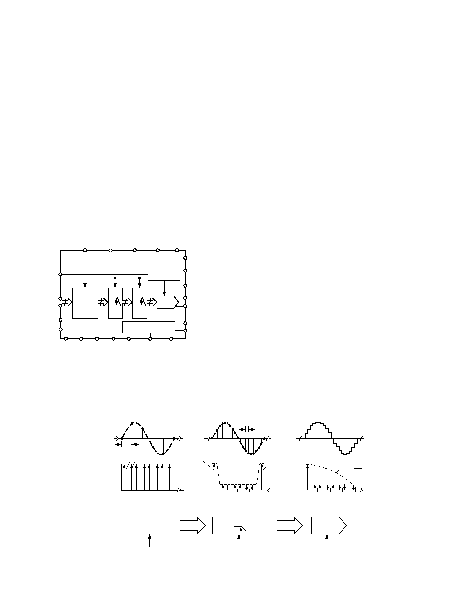
The benefits of an interpolation filter are clearly seen in Figure
23, which shows an example of the frequency and time domain
representation of a discrete time sine wave signal before and
after it is applied to a digital interpolation filter. Images of the
sine wave signal appear around multiples of the DAC’s input
data rate as predicted by sampling theory. These undesirable
images will also appear at the output of a reconstruction DAC,
although modified by the DAC’s sin(x)/(x) roll-off response.
In many bandlimited applications, these images must be sup-
pressed by an analog filter following the DAC. The complexity
of this analog filter is typically determined by the proximity of
the desired fundamental to the first image and the required
amount of image suppression. Adding to the complexity of this
analog filter may be the requirement of compensating for the
DAC’s sin(x)/x response.
Referring to Figure 23, the “new” first image associated with the
DAC’s higher data rate after interpolation is “pushed” out fur-
ther relative to the input signal. The “old” first image associated
with the lower DAC data rate before interpolation is suppressed
by the digital filter. As a result, the transition band for the ana-
log reconstruction filter is increased, thus reducing the complex-
ity of the analog filter. Furthermore, the sin(x)/x roll-off over the
effective passband (i.e., dc to fCLOCK/2) is significantly reduced.
The AD9774 includes a PLL clock multiplier that produces the
necessary internally synchronized 1
×, 2× and 4× clocks for the
edge triggered latches, interpolation filters and DACs. The
PLL clock multiplier typically accepts an input data clock,
CLK IN/OUT, as its reference source. Alternatively, it can also
be configured using an external 4
× clock via CLK4×IN. The
PLLDIVIDE, VCO IN/EXT, PLLENABLE, and PLLLOCK
are control inputs/outputs used in the PLL clock generator.
Refer to the PLL CLOCK MULTIPLIER OPERATION sec-
tion for a detailed discussion on its operation.
The digital section of the AD9774 also includes several other
control inputs and outputs. The SLEEP and SNOOZE inputs
provide different power-saving modes as discussed in the
SLEEP and SNOOZE section.
FUNDAMENTAL
4fCLOCK
2fCLOCK
FREQUENCY DOMAIN
4fCLOCK
DACs
"SINX"
X
2fCLOCK
1
4
f
CLOCK
FUNDAMENTAL
DIGITAL
FILTER
SUPPRESSED
"OLD"
1ST IMAGE
"NEW"
1ST IMAGE
4fCLOCK
2fCLOCK
1
f
CLOCK
TIME DOMAIN
4x INTERPOLATION FILTER
INPUT DATA LATCH
DAC
4 fCLOCK
fCLOCK
4x
1ST IMAGE
Figure 23. Time and Frequency Domain Example of Digital Interpolation Filter
相关PDF资料 |
PDF描述 |
|---|---|
| AD9779ABSVZRL | DAC 16BIT 1.0GSPS 100-TQFP |
| AD977ABNZ | IC ADC 16BIT 200KSPS 20DIP |
| AD9781BCPZ | IC DAC 14BT 500MSPS LVDS 72LFCSP |
| AD9877ABSZ | IC PROCESSOR FRONT END 100MQFP |
| AD9878BSTZ | IC FRONT-END MIXED-SGNL 100-LQFP |
相关代理商/技术参数 |
参数描述 |
|---|---|
| AD9774EB | 制造商:AD 制造商全称:Analog Devices 功能描述:14-Bit, 32 MSPS TxDAC⑩ with 4x Interpolation Filters |
| AD9774-EB | 制造商:Analog Devices 功能描述: |
| AD9774-EBZ | 制造商:Analog Devices 功能描述:14-BIT 32 MSPS TXDAC W/4X INTERPOLATION - Bulk |
| AD9775 | 制造商:AD 制造商全称:Analog Devices 功能描述:14-Bit, 160 MSPS 2X/4X/8X Interpolating Dual TxDAC+ D/A Converter |
| AD9775BSV | 制造商:Analog Devices 功能描述:DAC 2-CH R-2R 14-bit 80-Pin TQFP EP 制造商:Rochester Electronics LLC 功能描述:14BIT 160 MSPS DUAL TXDAC+ D/A CONVERTER - Bulk 制造商:Analog Devices 功能描述:IC 14-BIT DAC |
发布紧急采购,3分钟左右您将得到回复。