参数资料
| 型号: | AD9774ASZRL |
| 厂商: | Analog Devices Inc |
| 文件页数: | 6/24页 |
| 文件大小: | 0K |
| 描述: | IC DAC 14BIT 32MSPS 44MQFP |
| 产品变化通告: | Product Discontinuance 27/Oct/2011 |
| 标准包装: | 800 |
| 系列: | TxDAC+® |
| 设置时间: | 35ns |
| 位数: | 14 |
| 数据接口: | 并联 |
| 转换器数目: | 1 |
| 电压电源: | 模拟和数字 |
| 功率耗散(最大): | 1.13W |
| 工作温度: | -40°C ~ 85°C |
| 安装类型: | 表面贴装 |
| 封装/外壳: | 44-QFP |
| 供应商设备封装: | 44-MQFP(10x10) |
| 包装: | 带卷 (TR) |
| 输出数目和类型: | 2 电流,单极;2 电流,双极 |
| 采样率(每秒): | 32M |
AD9774
–14–
REV. B
AD9774
AVDD
IOUTA
IOUTB
RLOAD
Figure 31. Equivalent Analog Output Circuit
IOUTA and IOUTB also have a negative and positive voltage
compliance range. The negative output compliance range of
–1.0 V is set by the breakdown limits of the CMOS process.
Operation beyond this maximum limit may result in a break-
down of the output stage and affect the reliability of the AD9774.
The positive output compliance range is slightly dependent on
the full-scale output current, IOUTFS. It degrades slightly from its
nominal 1.25 V for an IOUTFS = 20 mA to 1.00 V for an IOUTFS =
2 mA. Operation beyond the positive compliance range will
induce clipping of the output signal, which severely degrades
the AD9774’s linearity and distortion performance.
For applications requiring the optimum dc linearity, IOUTA
and/or IOUTB should be maintained at a virtual ground via an
I-V op amp configuration. Maintaining IOUTA and/or IOUTB
at a virtual ground keeps the output impedance of the AD9774
fixed, significantly reducing its effect on linearity. However, it
does not necessarily lead to the optimum distortion perfor-
mance due to limitations of the I-V op amp. Note that the
INL/DNL specifications for the AD9774 are measured in this
manner using IOUTA. In addition, these dc linearity specifi-
cations remain virtually unaffected over the specified power
supply range of 2.7 V to 5.5 V.
Operating the AD9774 with reduced voltage output swings at
IOUTA and IOUTB in a differential or single-ended output
configuration reduces the signal dependency of its output im-
pedance thus enhancing distortion performance. Although the
voltage compliance range of IOUTA and IOUTB extends from
–1.0 V to +1.25 V, optimum distortion performance is achieved
when the maximum full-scale signal at IOUTA and IOUTB
does not exceed approximately 0.5 V. A properly selected trans-
former with a grounded center-tap will allow the AD9774 to
provide the required power and voltage levels to different loads
while maintaining reduced voltage swings at IOUTA and
IOUTB. DC-coupled applications requiring a differential or
single-ended output configuration should size RLOAD accord-
ingly. Refer to Applying the AD9774 section for examples of
various output configurations.
The most significant improvement in the AD9774’s distortion
and noise performance is realized using a differential output
configuration. The common-mode error sources of both IOUTA
and IOUTB can be substantially reduced by the common-mode
rejection of a transformer or differential amplifier. These
common-mode error sources include even-order distortion
products and noise. The enhancement in distortion performance
becomes more significant as the reconstructed waveform’s
frequency content increases and/or its amplitude decreases.
The distortion and noise performance of the AD9774 is also
slightly dependent on the analog and digital supply as well as the
full-scale current setting, IOUTFS. Operating the analog supply at
5.0 V ensures maximum headroom for its internal PMOS current
sources and differential switches leading to improved distortion
performance. Although IOUTFS can be set between 2 mA and
20 mA, selecting an IOUTFS of 20 mA will provide the best dis-
tortion and noise performance. The noise performance of the
AD9774 is affected by the digital supply (DVDD), output fre-
quency, and increases with increasing clock rate. Operating the
AD9774 with low voltage logic levels between 3 V and 3.3 V
will slightly reduce the amount of on-chip digital noise.
In summary, the AD9774 achieves the optimum distortion and
noise performance under the following conditions:
(1) Differential Operation.
(2) Positive voltage swing at IOUTA and IOUTB limited to
+0.5 V.
(3) IOUTFS set to 20 mA.
(4) Analog Supply (AVDD) set at 5.0 V.
(5) Digital Supply (DVDD) and Phase Lock Loop Supply
(PLLVDD) set at 3.0 V to 3.3 V with appropriate logic
levels.
Note that the ac performance of the AD9774 is characterized
under the above-mentioned operating conditions.
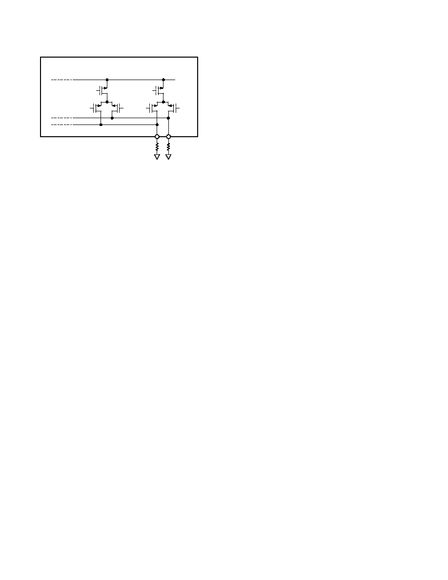
DIGITAL INPUTS/OUTPUTS
The digital input of the AD9774 consists of 14 data input pins
and a clock input pin, and several control input pins. Since
some of the internal logic is operated from DVDD and PLLVDD,
they must be set to the same or similar levels to ensure proper
compatibility with any external logic/drivers. The two digital
outputs of the AD9774, PLL LOCK and CLK OUT originate
from the internal PLL circuitry and thus its output logic levels
will be set by PLLVDD.
The 14-bit parallel data inputs follow standard positive binary
coding where DB13 is the most significant bit (MSB), and DB0
is the least significant bit (LSB). IOUTA produces a full-scale
output current when all data bits are at Logic 1. IOUTB pro-
duces a complementary output with the full-scale current split
between the two outputs as a function of the input code.
The digital interface is implemented using an edge-triggered
master slave latch and is designed to support a clock and input
data rate as high as 32 MSPS. The clock can be operated at any
duty cycle that meets the specified latch pulsewidth as shown in
Figure 1. The setup and hold times can also be varied within the
clock cycle as long as the specified minimum times are met.
The digital inputs are CMOS-compatible with logic thresholds,
VTHRESHOLD, set to approximately half the digital positive supply
(i.e., DVDD or PLLVDD) or
VTHRESHOLD = DVDD/2 (± 20%)
The internal digital circuitry of the AD9774 is capable of operating
over a digital supply range of 2.7 V to 5.5 V. As a result, the
digital inputs can also accommodate TTL levels when DVDD is
set to accommodate the maximum high level voltage of the TTL
drivers VOH(MAX). A DVDD of 3 V to 3.3 V will typically ensure
proper compatibility with most TTL logic families. Figure 32
shows the equivalent digital input circuit for the data and clock
inputs.
相关PDF资料 |
PDF描述 |
|---|---|
| AD9779ABSVZRL | DAC 16BIT 1.0GSPS 100-TQFP |
| AD977ABNZ | IC ADC 16BIT 200KSPS 20DIP |
| AD9781BCPZ | IC DAC 14BT 500MSPS LVDS 72LFCSP |
| AD9877ABSZ | IC PROCESSOR FRONT END 100MQFP |
| AD9878BSTZ | IC FRONT-END MIXED-SGNL 100-LQFP |
相关代理商/技术参数 |
参数描述 |
|---|---|
| AD9774EB | 制造商:AD 制造商全称:Analog Devices 功能描述:14-Bit, 32 MSPS TxDAC⑩ with 4x Interpolation Filters |
| AD9774-EB | 制造商:Analog Devices 功能描述: |
| AD9774-EBZ | 制造商:Analog Devices 功能描述:14-BIT 32 MSPS TXDAC W/4X INTERPOLATION - Bulk |
| AD9775 | 制造商:AD 制造商全称:Analog Devices 功能描述:14-Bit, 160 MSPS 2X/4X/8X Interpolating Dual TxDAC+ D/A Converter |
| AD9775BSV | 制造商:Analog Devices 功能描述:DAC 2-CH R-2R 14-bit 80-Pin TQFP EP 制造商:Rochester Electronics LLC 功能描述:14BIT 160 MSPS DUAL TXDAC+ D/A CONVERTER - Bulk 制造商:Analog Devices 功能描述:IC 14-BIT DAC |
发布紧急采购,3分钟左右您将得到回复。