- 您现在的位置:买卖IC网 > PDF目录16826 > AD9858/PCBZ (Analog Devices Inc)BOARD EVAL FOR AD9858 PDF资料下载
参数资料
| 型号: | AD9858/PCBZ |
| 厂商: | Analog Devices Inc |
| 文件页数: | 13/32页 |
| 文件大小: | 0K |
| 描述: | BOARD EVAL FOR AD9858 |
| 产品培训模块: | Direct Digital Synthesis Tutorial Series (1 of 7): Introduction Direct Digital Synthesizer Tutorial Series (7 of 7): DDS in Action Direct Digital Synthesis Tutorial Series (3 of 7): Angle to Amplitude Converter Direct Digital Synthesis Tutorial Series (6 of 7): SINC Envelope Correction Direct Digital Synthesis Tutorial Series (4 of 7): Digital-to-Analog Converter Direct Digital Synthesis Tutorial Series (2 of 7): The Accumulator |
| 设计资源: | Low Jitter Sampling Clock Generator for High Performance ADCs Using AD9958/9858 and AD9515 (CN0109) |
| 标准包装: | 1 |
| 主要目的: | 计时,直接数字合成(DDS) |
| 已用 IC / 零件: | AD9858/TL |
| 已供物品: | 板 |
| 其它名称: | AD9858/PCB AD9858/PCB-ND |
第1页第2页第3页第4页第5页第6页第7页第8页第9页第10页第11页第12页当前第13页第14页第15页第16页第17页第18页第19页第20页第21页第22页第23页第24页第25页第26页第27页第28页第29页第30页第31页第32页
AD9858
Rev. C | Page 20 of 32
I/O Port Functionality
The I/O port can operate in either serial or parallel programming
mode. Mode selection is accomplished via the SPSELECT pin.
The ability to read back the contents of a register is provided in
both modes to facilitate the debug process during the user’s
prototyping phase of a design. In either mode, however, the
reading back of profile registers requires that the profile select
pins (PS0 and PS1) be configured to select the desired register
bank. When reading a register that resides in one of the profiles,
the register address acts as an offset to select one of the registers
among the group of registers defined by the profile. The profile
select pins control the base address of the register bank and
select the appropriate register grouping.
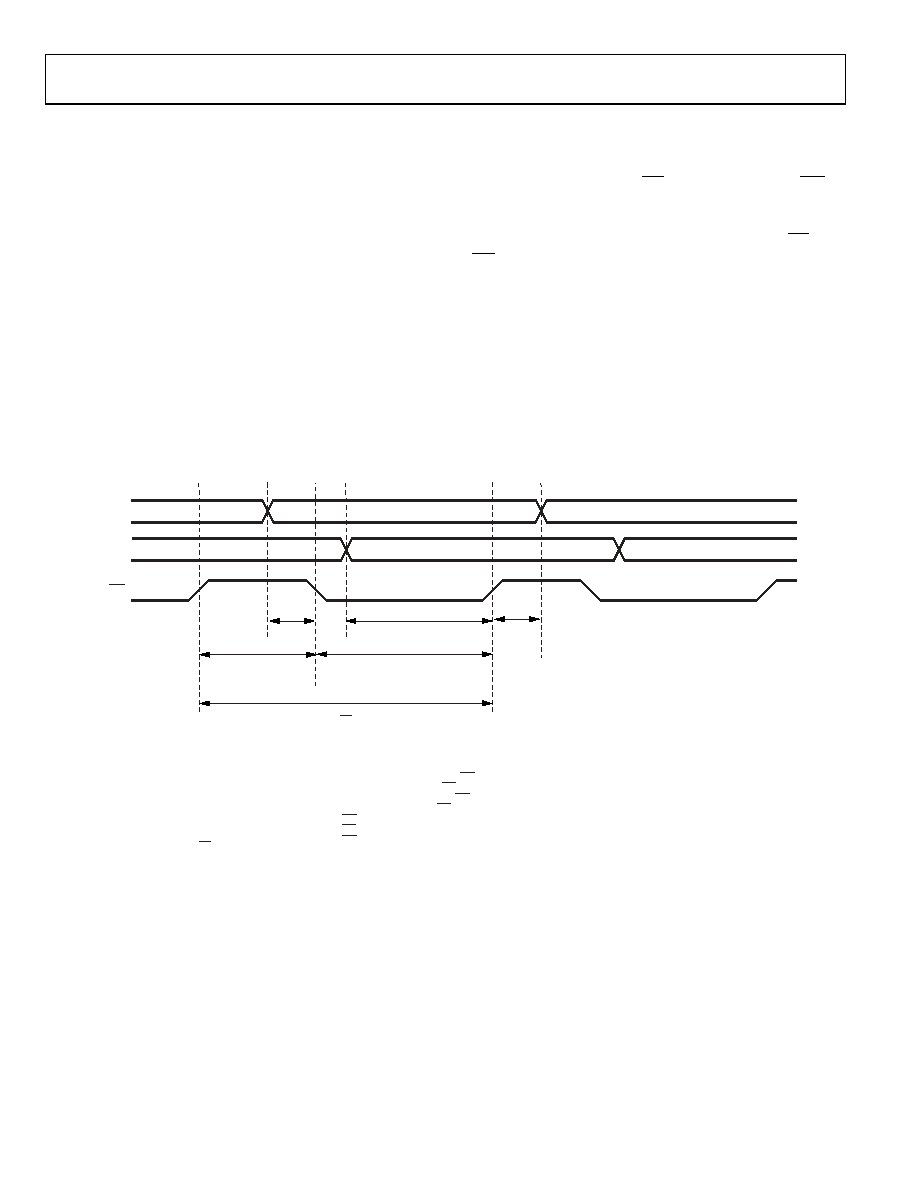
Parallel Programming Mode
In parallel programming mode, the I/O port makes use of eight
bidirectional data pins (D7 to D0), six address input pins (ADDR5
to ADDR0), a read input pin (RD), and a write input pin (WR).
A register is selected by providing the proper address combination
as defined in the register map (see
). Read or write
functionality is invoked by pulsing the appropriate pin (
RD or
WR); the two operations are mutually exclusive. The read or write
data is transported on the D7 to D0 pins. The correlation between
the D7 to D0 data bits and their functionality at a specific register
address is detailed in the register map (see
) and register
bit description.
Parallel I/O operation allows write access to each byte of any
register in the I/O buffer memory in a single I/O operation.
Readback capability is slower than write capability. It is intended as
a low speed function for debug purposes. Timing for both write
and read cycles is depicted in Figure 35 and Figure 36.
A3
A1
A2
D3
D1
D2
tWRHIGH
tWRLOW
tAHU
tDHU
tDSU
tASU
tWR
tASU
tDSU
tAHU
tDHU
tWRLOW
tWRHIGH
tWR
SPECIFICATION
3ns
3.5ns
0ns
3ns
6ns
9ns
VALUE
ADDRESS SETUP TIME TO WR SIGNAL ACTIVE
DATA SETUP TIME TO WR SIGNAL INACTIVE
ADDRESS HOLD TIME TO WR SIGNAL INACTIVE
DATA HOLD TIME TO WR SIGNAL INACTIVE
WR SIGNAL MINIMUM LOW TIME
WR SIGNAL MINIMUM HIGH TIME
WR SIGNAL MINIMUM PERIOD
DESCRIPTION
D[7:0]
ADDR[5:0]
WR
03
16
6-
03
8
Figure 35. I/O Port Write Cycle Timing (Parallel)
相关PDF资料 |
PDF描述 |
|---|---|
| AD9956-VCO/PCBZ | BOARD EVAL 14BIT 1.8V 48LFCSP |
| GEM22DRKF | CONN EDGECARD 44POS DIP .156 SLD |
| 362A024-4/86-0 | BOOT MOLDED |
| AD9956/PCBZ | BOARD EVAL FOR AD9956 |
| 0210391089 | CABLE JUMPER 1MM .203M 37POS |
相关代理商/技术参数 |
参数描述 |
|---|---|
| AD9858TLPCB | 制造商:AD 制造商全称:Analog Devices 功能描述:1 GSPS Direct Digital Synthesizer |
| AD9858XSV | 制造商:Analog Devices 功能描述: |
| AD9859 | 制造商:AD 制造商全称:Analog Devices 功能描述:400 MSPS, 10-Bit, 1.8 V CMOS Direct Digital Synthesizer |
| AD9859/PCB | 制造商:Analog Devices 功能描述:NCO, 400MSPS 10 BIT, 1.8V CMOS DIRECT DGTL SYNTHESIZER - Bulk |
| AD9859/PCBZ | 功能描述:BOARD EVAL FOR AD9859 RoHS:是 类别:编程器,开发系统 >> 评估演示板和套件 系列:AgileRF™ 标准包装:1 系列:- 主要目的:电信,线路接口单元(LIU) 嵌入式:- 已用 IC / 零件:IDT82V2081 主要属性:T1/J1/E1 LIU 次要属性:- 已供物品:板,电源,线缆,CD 其它名称:82EBV2081 |
发布紧急采购,3分钟左右您将得到回复。