- 您现在的位置:买卖IC网 > PDF目录16826 > AD9858/PCBZ (Analog Devices Inc)BOARD EVAL FOR AD9858 PDF资料下载
参数资料
| 型号: | AD9858/PCBZ |
| 厂商: | Analog Devices Inc |
| 文件页数: | 14/32页 |
| 文件大小: | 0K |
| 描述: | BOARD EVAL FOR AD9858 |
| 产品培训模块: | Direct Digital Synthesis Tutorial Series (1 of 7): Introduction Direct Digital Synthesizer Tutorial Series (7 of 7): DDS in Action Direct Digital Synthesis Tutorial Series (3 of 7): Angle to Amplitude Converter Direct Digital Synthesis Tutorial Series (6 of 7): SINC Envelope Correction Direct Digital Synthesis Tutorial Series (4 of 7): Digital-to-Analog Converter Direct Digital Synthesis Tutorial Series (2 of 7): The Accumulator |
| 设计资源: | Low Jitter Sampling Clock Generator for High Performance ADCs Using AD9958/9858 and AD9515 (CN0109) |
| 标准包装: | 1 |
| 主要目的: | 计时,直接数字合成(DDS) |
| 已用 IC / 零件: | AD9858/TL |
| 已供物品: | 板 |
| 其它名称: | AD9858/PCB AD9858/PCB-ND |
第1页第2页第3页第4页第5页第6页第7页第8页第9页第10页第11页第12页第13页当前第14页第15页第16页第17页第18页第19页第20页第21页第22页第23页第24页第25页第26页第27页第28页第29页第30页第31页第32页
AD9858
Rev. C | Page 21 of 32
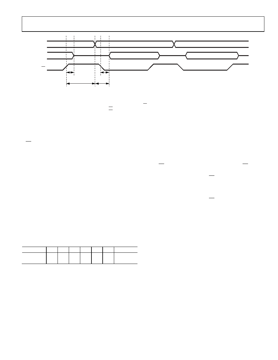
A3
A1
A2
D3
D1
D2
tRDHOZ
tRDLOV
tADV
tAHD
tADV
tAHD
tRDLOV
tRDHOZ
SPECIFICATION
15ns
5ns
15ns
10ns
VALUE
ADDRESS TO DATA VALID TIME (MAXIMUM)
ADDRESS HOLD TIME TO RD SIGNAL INACTIVE (MINIMUM)
RD LOW TO OUTPUT VALID (MAXIMUM)
RD HIGH TO DATA THREE-STATE (MAXIMUM)
DESCRIPTION
RD
ADDR[5:0]
D[7:0]
0
3
166
-03
9
Figure 36. I/O Port Read Cycle Timing (Parallel)
Serial Programming Mode
In serial programming mode, the I/O port uses a chip select pin
(CS), a serial clock pin (SCLK), an I/O reset pin (IORESET),
and either one or two serial data pins (SDIO and/or SDO). The
number of serial data pins used depends on the configuration of
the I/O port, that is, whether it has been configured for 2-wire
or 3-wire serial operation as defined by the control function
register. In 2-wire mode, the SDIO pin operates as a bidirectional
serial data pin. In 3-wire mode, the SDIO pin operates as a
serial data input pin only, and the SDO pin acts as the serial
output. The maximum rate of SCLK is guaranteed only for write
operation.
The serial port is an SPI-compatible serial interface. Serial port
communication occurs in two phases. Phase 1 is an instruction
cycle consisting of an 8-bit word. The MSB of the instruction
byte flags the ensuing operation as a read or write operation.
The six LSBs define the serial address of the target register as
defined in the register map. The instruction byte format is given in
Table 5.
D7 (MSB)
D6
D5
D4
D3
D2
D1
D0 (LSB)
1: Read
X
A5
A4
A3
A2
A1
A0
0: Write
Phase 2 of a serial port communication contains the data to be
routed to/from the addressed register. The number of bytes
transferred during Phase 2 depends on the length of the target
register. Serial operation requires that all bits associated with a
serial register address be transferred.
Both phases of a serial port communication require the serial
data clock (SCLK) to be operating. When writing to the device,
serial bits are transferred on the rising edge of SCLK. When
reading from the device, serial output bits are transferred on the
falling edge of SCLK. The bit order for both phases of a serial
port communication is selectable via the control function register.
The CS pin serves as a chip select control line. When CS is in a
Logic 1 state, the SDO and SDIO pins are disabled (forced into a
high impedance state). When the CS pin is in a Logic 0 state,
the SDO and SDIO pins are active. This allows multiple devices
to reside on a single serial bus. If multiple devices are connected
to the same serial bus, then communication with an individual
device is accomplished by setting CS to a Logic 0 state on the
target device, but to a Logic 1 state on all other devices. In this
way, serial communication occurs only between the controller
and the target device.
When I/O synchronization is lost between the AD9858 and
the external controller, the IORESET pin provides a means
to reestablish synchronization without initializing the entire
device. Asserting the active high IORESET pin resets the serial
port state machine. This terminates the current I/O operation
and puts the device into a state in which the next eight SCLK
pulses are expected to be the instruction byte of the next I/O
transfer. Any information previously written to the memory
registers during the last valid communication cycle prior to loss
of synchronization remains intact.
相关PDF资料 |
PDF描述 |
|---|---|
| AD9956-VCO/PCBZ | BOARD EVAL 14BIT 1.8V 48LFCSP |
| GEM22DRKF | CONN EDGECARD 44POS DIP .156 SLD |
| 362A024-4/86-0 | BOOT MOLDED |
| AD9956/PCBZ | BOARD EVAL FOR AD9956 |
| 0210391089 | CABLE JUMPER 1MM .203M 37POS |
相关代理商/技术参数 |
参数描述 |
|---|---|
| AD9858TLPCB | 制造商:AD 制造商全称:Analog Devices 功能描述:1 GSPS Direct Digital Synthesizer |
| AD9858XSV | 制造商:Analog Devices 功能描述: |
| AD9859 | 制造商:AD 制造商全称:Analog Devices 功能描述:400 MSPS, 10-Bit, 1.8 V CMOS Direct Digital Synthesizer |
| AD9859/PCB | 制造商:Analog Devices 功能描述:NCO, 400MSPS 10 BIT, 1.8V CMOS DIRECT DGTL SYNTHESIZER - Bulk |
| AD9859/PCBZ | 功能描述:BOARD EVAL FOR AD9859 RoHS:是 类别:编程器,开发系统 >> 评估演示板和套件 系列:AgileRF™ 标准包装:1 系列:- 主要目的:电信,线路接口单元(LIU) 嵌入式:- 已用 IC / 零件:IDT82V2081 主要属性:T1/J1/E1 LIU 次要属性:- 已供物品:板,电源,线缆,CD 其它名称:82EBV2081 |
发布紧急采购,3分钟左右您将得到回复。