- 您现在的位置:买卖IC网 > PDF目录11804 > AD9887AKSZ-170 (Analog Devices Inc)IC INTRFACE ANALOG/DVI 160-MQFP PDF资料下载
参数资料
| 型号: | AD9887AKSZ-170 |
| 厂商: | Analog Devices Inc |
| 文件页数: | 18/40页 |
| 文件大小: | 0K |
| 描述: | IC INTRFACE ANALOG/DVI 160-MQFP |
| 标准包装: | 24 |
| 应用: | 图形卡,VGA 接口 |
| 接口: | 模拟和数字 |
| 电源电压: | 3.15 V ~ 3.45 V |
| 封装/外壳: | 160-BQFP |
| 供应商设备封装: | 160-MQFP(28x28) |
| 包装: | 托盘 |
| 安装类型: | 表面贴装 |
| 产品目录页面: | 788 (CN2011-ZH PDF) |
第1页第2页第3页第4页第5页第6页第7页第8页第9页第10页第11页第12页第13页第14页第15页第16页第17页当前第18页第19页第20页第21页第22页第23页第24页第25页第26页第27页第28页第29页第30页第31页第32页第33页第34页第35页第36页第37页第38页第39页第40页
REV. 0
AD9887
–25–
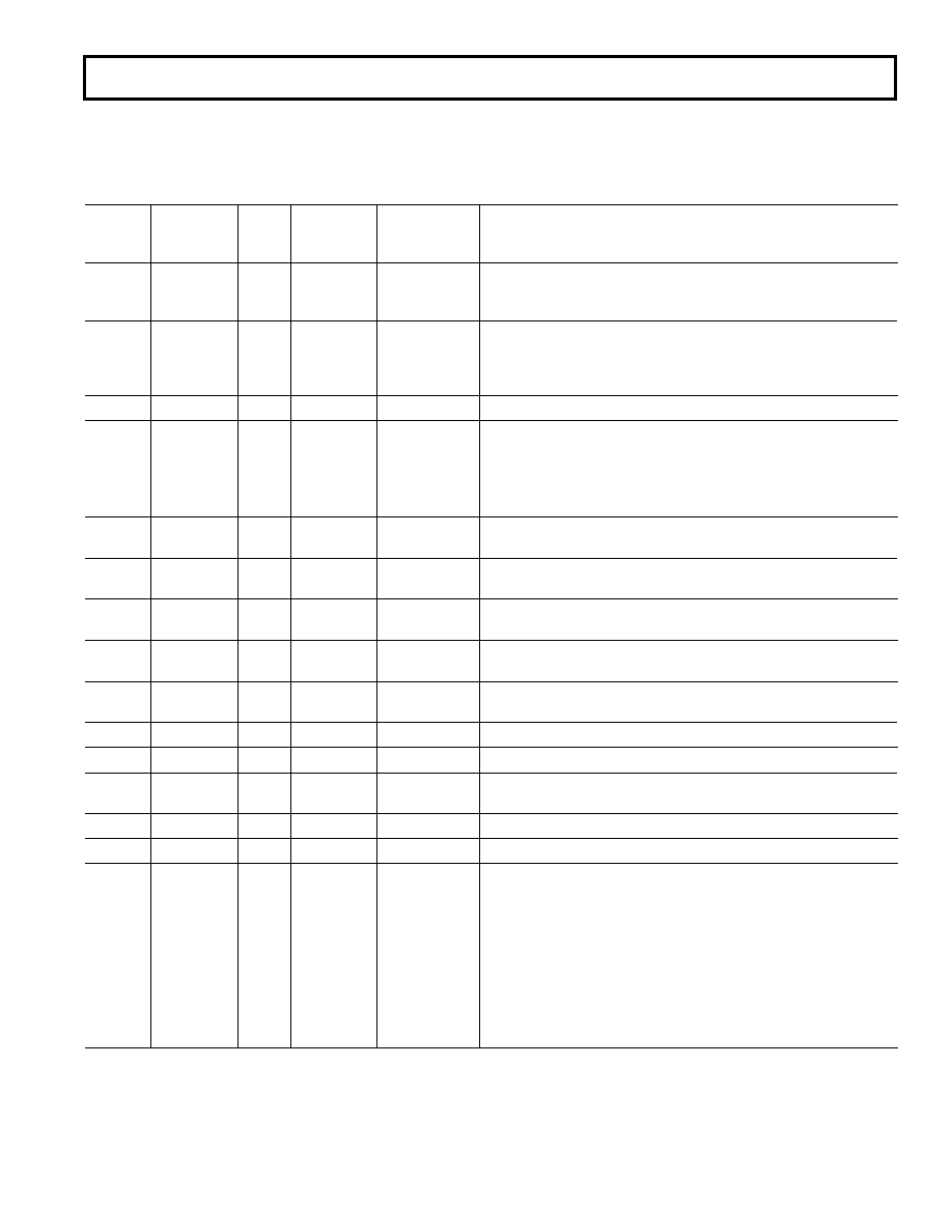
2-Wire Serial Register Map
The AD9887 is initialized and controlled by a set of registers, which determine the operating modes. An external controller is
employed to write and read the Control Registers through the 2-line serial interface port.
Table IX. Control Register Map
Read and
Hex
Write or
Default
Register
Address
Read Only
Bits
Value
Name
Function
00H
RO
7:0
Chip Revision
Bits 7 through 4 represent functional revisions to the analog interface.
Bits 3 through 0 represent nonfunctional related revisions.
Revision 0 = 0000 0000
01H
R/
W
7:0
01101001
PLL Div MSB
This register is for Bits [11:4] of the PLL divider. Larger values mean
the PLL operates at a faster rate. This register should be loaded rst
whenever a change is needed. (This will give the PLL more time to
lock.) See Note 1.
02H
R/
W
7:4
1101
****
PLL Div LSB
Bits [7:4] LSBs of the PLL divider word. See Note 1.
03H
R/
W
7:2
1
*******
VCO/CPMP
Bit 7—Must be set to 1 for proper device operation.
*01*****
Bits [6:5] VCO Range. Selects VCO frequency range. (See PLL
description.)
***001**
Bits [4:2] Charge Pump Current. Varies the current that drives the
low-pass lter. (See PLL description.)
04H
R/
W
7:3
10000
***
Phase Adjust
ADC Clock phase adjustment. Larger values mean more delay.
(1 LSB = T/32)
05H
R/
W
7:0
10000000
Clamp
Places the Clamp signal an integer number of clock periods after the trail-
Placement
ing edge of the Hsync signal.
06H
R/
W
7:0
10000000
Clamp
Number of clock periods that the Clamp signal is actively clamping.
Duration
07H
R/
W
7:0
00100000
Hsync Output
Sets the number of pixel clocks that HSOUT will remain active.
Pulsewidth
08H
R/
W
7:0
10000000
Red Gain
Controls ADC input range (Contrast) of each respective channel.
Bigger values give less contrast.
09H
R/
W
7:0
10000000
Green Gain
0AH
R/
W
7:0
10000000
Blue Gain
0BH
R/
W
7:1
1000000
*
Red Offset
Controls dc offset (Brightness) of each respective channel. Bigger
values decrease brightness.
0CH
R/
W
7:1
1000000
*
Green Offset
0DH
R/
W
7:1
1000000
*
Blue Offset
0EH
R/
W
7:3
1
*******
Mode
Bit 7—Channel Mode. Determines Single Channel or Dual Channel
Control 1
Output Mode. (Logic 0 = Single Channel Mode, Logic 1 = Dual
Channel Mode.)
*1******
Bit 6—Output Mode. Determine Interleaved or Parallel Output Mode.
(Logic 0 = Interleaved Mode, Logic 1 = Parallel Mode.)
**0*****
Bit 5—OUTPHASE. Determines which port outputs the rst data byte
after Hsync. (Logic 0 = B Port, Logic 1 = A Port.)
***0****
Bit 4—Hsync Output polarity. (Logic 0 = Logic High Sync, Logic 1 =
Logic Low Sync.)
****0***
Bit 3—Vsync Output Invert. (Logic 0 = Invert, Logic 1 = No Invert.)
OBSOLETE
相关PDF资料 |
PDF描述 |
|---|---|
| VE-B5T-IX-F2 | CONVERTER MOD DC/DC 6.5V 75W |
| VE-B5T-IX-F1 | CONVERTER MOD DC/DC 6.5V 75W |
| AT89C51CC03C-RDRIM | IC 8051 MCU FLASH 64K 64VQFP |
| D38999/24FC8SN | CONN RCPT 8POS JAM NUT W/SCKT |
| MS27473T18A35S | CONN PLUG 66POS STRAIGHT W/SCKT |
相关代理商/技术参数 |
参数描述 |
|---|---|
| AD9887AKSZ-170 | 制造商:Analog Devices 功能描述:IC DUAL DISPLAY INTERFACE |
| AD9887AKSZ-1701 | 制造商:AD 制造商全称:Analog Devices 功能描述:Dual Interface for Flat Panel Display |
| AD9887APCB | 制造商:AD 制造商全称:Analog Devices 功能描述:Dual Interface for Flat Panel Displays |
| AD9887KS-100 | 制造商:Analog Devices 功能描述:Interface for Flat Panel Display 160-Pin MQFP 制造商:Rochester Electronics LLC 功能描述:DUAL A/D INTERFACE FOR FLAT PANEL - Bulk |
| AD9887KS-140 | 制造商:Analog Devices 功能描述:Interface for Flat Panel Display 160-Pin MQFP 制造商:Rochester Electronics LLC 功能描述:DUAL A/D INTERFACE FOR FLAT PANEL - Bulk 制造商:Analog Devices 功能描述:IC INTERFACE DUAL DISPLAY |
发布紧急采购,3分钟左右您将得到回复。