- 您现在的位置:买卖IC网 > PDF目录1894 > AD9888KSZ-170 (Analog Devices Inc)IC ANALOG INTRFC 170MSPS 128MQFP PDF资料下载
参数资料
| 型号: | AD9888KSZ-170 |
| 厂商: | Analog Devices Inc |
| 文件页数: | 7/36页 |
| 文件大小: | 0K |
| 描述: | IC ANALOG INTRFC 170MSPS 128MQFP |
| 标准包装: | 1 |
| 应用: | 图形卡,VGA 接口 |
| 接口: | 2 线串口 |
| 电源电压: | 3 V ~ 3.6 V |
| 封装/外壳: | 128-BFQFP |
| 供应商设备封装: | 128-MQFP(14x20) |
| 包装: | 托盘 |
| 安装类型: | 表面贴装 |
第1页第2页第3页第4页第5页第6页当前第7页第8页第9页第10页第11页第12页第13页第14页第15页第16页第17页第18页第19页第20页第21页第22页第23页第24页第25页第26页第27页第28页第29页第30页第31页第32页第33页第34页第35页第36页
Data Sheet
AD9888
Rev. C | Page 15 of 36
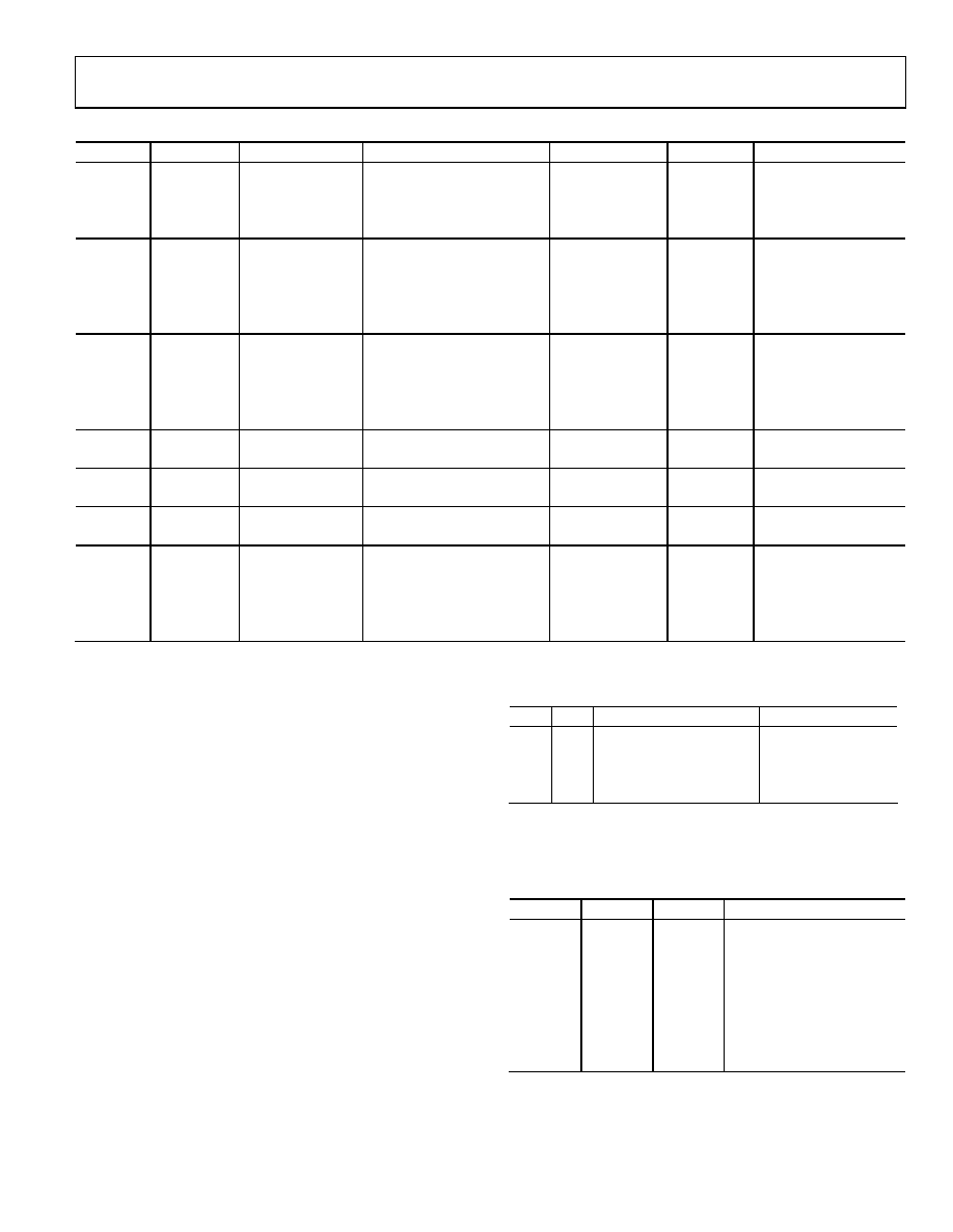
Table 5. Recommended VCO Range and Charge Pump Current Settings for Standard Display Formats
Standard
Resolution
Refresh Rate (Hz)
Horizontal Frequency (kHz)
Pixel Rate (MHz)
VCO Range
Charge Pump Current
VGA
640 × 480
60
31.5
25.175
00
010
72
37.7
31.500
00
100
75
37.5
31.500
00
100
85
43.3
36.000
00
100
SVGA
800 × 600
56
35.1
36.000
00
100
60
37.9
40.000
00
101
72
48.1
50.000
01
011
75
46.9
49.500
01
011
85
53.7
56.250
01
011
XGA
1024 × 768
60
48.4
65.000
01
100
70
56.5
75.000
01
100
75
60.0
78.750
01
101
80
64.0
85.500
10
011
85
68.3
94.500
10
011
SXGA
1280 × 1024
64.0
108.000
10
011
80.0
135.000
10
100
UXGA
1600 × 1200
60
75.0
162.000
11
100
85
106.3
229.5001
10
110
QXGA
2048 × 1536
60
96.8
260.0001
11
100
2048 × 1536
75
120.0
315.0001
11
100
TV Modes
480i
60
15.75
13.510
00
000
480p
60
31.47
27.000
00
011
720p
60
45.0
74.250
01
011
1080i
60
33.75
74.250
01
011
1080p
60
33.75
148.500
10
011
1 Graphics sampled at half the incoming pixel rate using alternate pixel sampling mode.
Four programmable registers are provided to optimize the
performance of the PLL:
The 12-bit divisor registers. The input HSYNC frequencies
range from 15 kHz to 110 kHz. The PLL multiplies the
frequency of the HSYNC signal, producing pixel clock
frequencies in the range of 10 MHz to 170 MHz. The
divisor register controls the exact multiplication factor.
This register can be set to any value between 221 and 4095.
(The divide ratio that is actually used is the programmed
divide ratio plus one.)
The 2-bit VCO range register. To lower the sensitivity of
the output frequency to noise on the control signal, the
VCO operating frequency range is divided into four
overlapping regions. The VCO range register sets this
operating range. Because there are just four possible
regions, only the two least significant bits of the VCO
range register are used. The frequency ranges for the
lowest and highest regions are shown in Table 6.
Table 6. VCO Frequency Ranges
PV1
PV0
Pixel Clock Range (MHz)
KVCO Gain (MHz/V)
0
10 to 41
150
0
1
41 to 82
150
1
0
82 to 150
150
1
150+
180
The 3-bit charge pump current register. This register allows
the current that drives the low-pass loop filter to be varied.
The possible current values are listed in Table 7.
Table 7. Charge Pump Current/Control Bits
Ip2
Ip1
Ip0
Current (μA)
0
50
0
1
100
0
1
0
150
0
1
250
1
0
350
1
0
1
500
1
0
750
1
1500
相关PDF资料 |
PDF描述 |
|---|---|
| AD9895KBCZRL | IC CCD SIGNAL PROC/GEN 64-CSPBGA |
| AD9910BSVZ-REEL | IC DDS 1GSPS 14BIT PAR 100TQFP |
| AD9911BCPZ-REEL7 | IC DDS 500MSPS DAC 10BIT 56LFCSP |
| AD9912ABCPZ | IC DDS 1GSPS DAC 14BIT 64LFCSP |
| AD9913BCPZ-REEL7 | IC DDS 250MSPS 10BIT ADC 32LFCSP |
相关代理商/技术参数 |
参数描述 |
|---|---|
| AD9888KSZ-170 | 制造商:Analog Devices 功能描述:TV / Video IC |
| AD9888KSZ-205 | 制造商:Analog Devices 功能描述:205MHZ ANALOG GRAPHICS INTERFACE 制造商:Analog Devices 功能描述:IC ANALOG INTERFACE |
| AD9888KSZ-205KL1 | 制造商:Analog Devices 功能描述:- Rail/Tube |
| AD9889 | 制造商:Analog Devices 功能描述:- Bulk |
| AD9889A | 制造商:AD 制造商全称:Analog Devices 功能描述:High Performance HDMI/DVI Transmitter |
发布紧急采购,3分钟左右您将得到回复。