- 您现在的位置:买卖IC网 > PDF目录10979 > AD9959BCPZ (Analog Devices Inc)IC DDS QUAD 10BIT DAC 56LFCSP PDF资料下载
参数资料
| 型号: | AD9959BCPZ |
| 厂商: | Analog Devices Inc |
| 文件页数: | 13/44页 |
| 文件大小: | 0K |
| 描述: | IC DDS QUAD 10BIT DAC 56LFCSP |
| 产品培训模块: | Direct Digital Synthesis Tutorial Series (1 of 7): Introduction Direct Digital Synthesizer Tutorial Series (7 of 7): DDS in Action Direct Digital Synthesis Tutorial Series (3 of 7): Angle to Amplitude Converter Direct Digital Synthesis Tutorial Series (6 of 7): SINC Envelope Correction Direct Digital Synthesis Tutorial Series (4 of 7): Digital-to-Analog Converter Direct Digital Synthesis Tutorial Series (2 of 7): The Accumulator |
| 设计资源: | Phase Coherent FSK Modulator (CN0186) |
| 标准包装: | 1 |
| 分辨率(位): | 10 b |
| 主 fclk: | 500MHz |
| 调节字宽(位): | 32 b |
| 电源电压: | 1.71 V ~ 1.96 V |
| 工作温度: | -40°C ~ 85°C |
| 安装类型: | 表面贴装 |
| 封装/外壳: | 56-VFQFN 裸露焊盘,CSP |
| 供应商设备封装: | 56-LFCSP-VQ(8x8) |
| 包装: | 托盘 |
| 产品目录页面: | 552 (CN2011-ZH PDF) |
第1页第2页第3页第4页第5页第6页第7页第8页第9页第10页第11页第12页当前第13页第14页第15页第16页第17页第18页第19页第20页第21页第22页第23页第24页第25页第26页第27页第28页第29页第30页第31页第32页第33页第34页第35页第36页第37页第38页第39页第40页第41页第42页第43页第44页
AD9959
Rev. B | Page 20 of 44
Single-Tone Mode—Matched Pipeline Delay
In single-tone mode, the AD9959 offers matched pipeline delay
to the DAC input for all frequency, phase, and amplitude changes.
This avoids having to deal with different pipeline delays between
the three input ports for such applications. The feature is enabled
by asserting the matched pipe delays active bit found in the
channel function register (CFR, Register 0x03). This feature
is available in single-tone mode only.
REFERENCE CLOCK MODES
The AD9959 supports multiple reference clock configurations
to generate the internal system clock. As an alternative to
clocking the part directly with a high frequency clock source,
the system clock can be generated using the internal, PLL-based
reference clock multiplier. An on-chip oscillator circuit is also
available for providing a low frequency reference signal by
connecting a crystal to the clock input pins. Enabling these
features allows the part to operate with a low frequency clock
source and still provide a high update rate for the DDS and
DAC. However, using the clock multiplier changes the output
phase noise characteristics. For best phase noise performance,
a clean, stable clock with a high slew is required (see Figure 17
and Figure 18).
Enabling the PLL allows multiplication of the reference clock
frequency from 4× to 20×, in integer steps. The PLL multiplica-
tion value is represented by a 5-bit multiplier value. These bits
are located in Function Register 1 (FR1, Register 0x01), Bits[22:18]
(see the Register Maps and Bit Descriptions section).
When FR1[22:18] is programmed with values ranging from
4 to 20 (decimal), the clock multiplier is enabled. The integer
value in the register represents the multiplication factor. The
system clock rate with the clock multiplier enabled is equal to
the reference clock rate multiplied by the multiplication factor.
If FR1[22:18] is programmed with a value less than 4 or greater
than 20, the clock multiplier is disabled and the multiplication
factor is effectively 1.
Whenever the PLL clock multiplier is enabled or the multiplica-
tion value is changed, time should be allowed to lock the PLL
(typically 1 ms).
Note that the output frequency of the PLL is restricted to a
frequency range of 100 MHz to 500 MHz. However, there is a
VCO gain control bit that must be used appropriately. The VCO
gain control bit defines two ranges (low/high) of frequency
output. The VCO gain control bit defaults to low (see Table 1
for details).
The charge pump current in the PLL defaults to 75 μA. This
setting typically produces the best phase noise characteristics.
Increasing the charge pump current may degrade phase noise,
but it decreases the lock time and changes the loop bandwidth.
Enabling the on-chip oscillator for crystal operation is performed
by driving CLK_MODE_SEL (Pin 24) to logic high (1.8 V
logic). With the on-chip oscillator enabled, connection of an
external crystal to the REF_CLK and REF_CLK inputs is made,
producing a low frequency reference clock. The frequency of
the crystal must be in the range of 20 MHz to 30 MHz.
for more details.
Reference Clock Input Circuitry
The reference clock input circuitry has two modes of operation
controlled by the logic state of Pin 24 (CLK_MODE_SEL). The
first mode (logic low) configures as an input buffer. In this
mode, the reference clock must be ac-coupled to the input due
to internal dc biasing. This mode supports either differential
or single-ended configurations. If single-ended mode is chosen,
the complementary reference clock input (Pin 22) should be
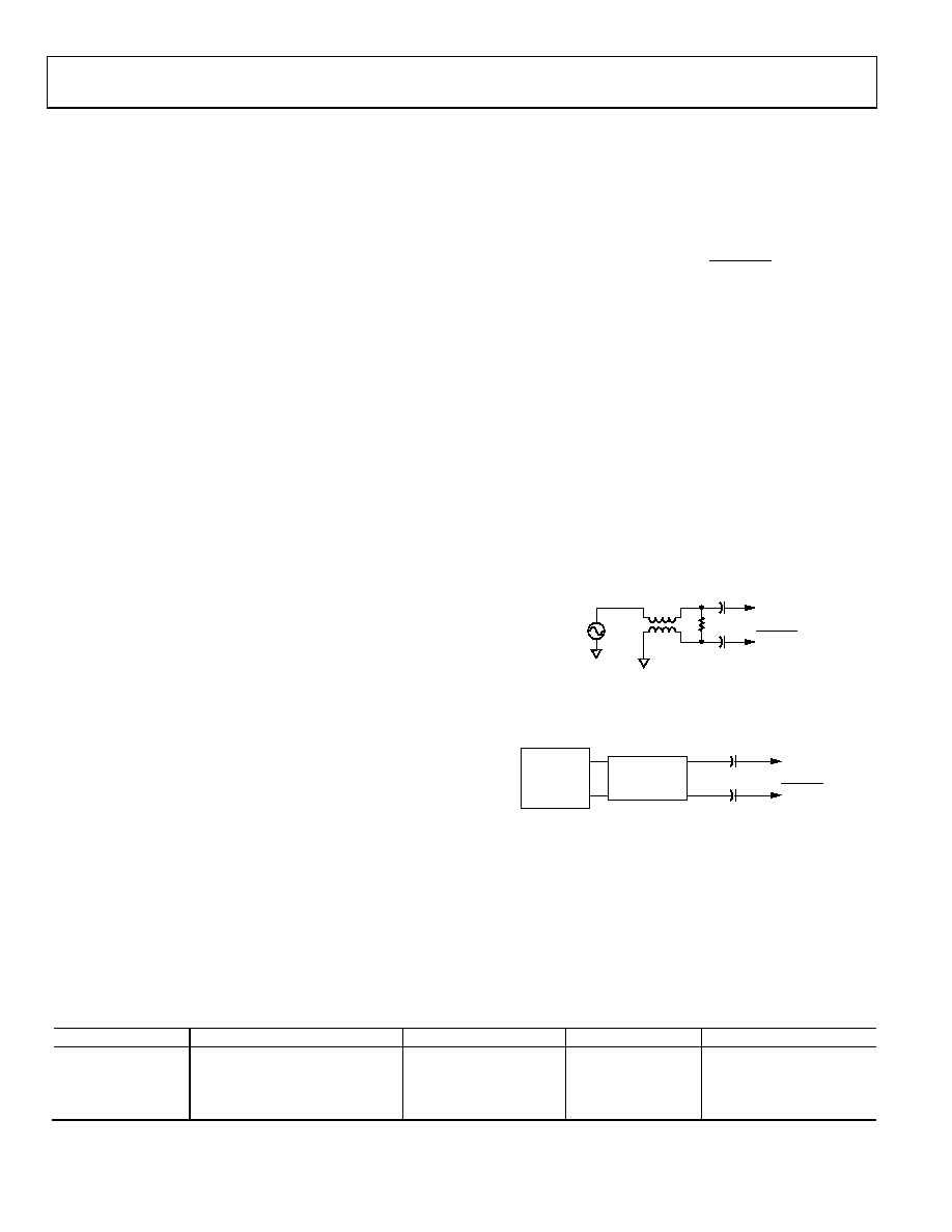
decoupled to AVDD or AGND via a 0.1 μF capacitor. Figure 33
to Figure 35 exemplify typical reference clock configurations for
the AD9959.
0
52
46
-017
1:1
BALUN
REF_CLK
PIN 23
REFCLK
SOURCE
REF_CLK
PIN 22
50
0.1F
Figure 33. Differential Coupling from Single-Ended Source
The reference clock inputs can also support an LVPECL or
PECL driver as the reference clock source.
05
24
6-
01
8
REF_CLK
PIN 23
REF_CLK
PIN 22
0.1F
LVPECL/
PECL
DRIVER
TERMINATION
Figure 34. Differential Clock Source Hook-Up
The second mode of operation (Pin 24 = logic high = 1.8 V)
provides an internal oscillator for crystal operation. In this
mode, both clock inputs are dc-coupled via the crystal leads
and are bypassed. The range of crystal frequencies supported is
from 20 MHz to 30 MHz. Figure 35 shows the configuration
for using a crystal.
Table 4. Clock Configuration
CLK_MODE_SEL, Pin 24
FR1[22:18] PLL Divider Ratio = M
Crystal Oscillator Enabled
System Clock (fSYSCLK)
Min/Max Freq. Range (MHz)
High = 1.8 V Logic
4 ≤ M ≤ 20
Yes
fSYSCLK = fOSC × M
100 < fSYSCLK < 500
High = 1.8 V Logic
M < 4 or M > 20
Yes
fSYSCLK = fOSC
20 < fSYSCLK < 30
Low
4 ≤ M ≤ 20
No
fSYSCLK = fREFCLK × M
100 < fSYSCLK < 500
Low
M < 4 or M > 20
No
fSYSCLK = fREFCLK
0 < fSYSCLK < 500
相关PDF资料 |
PDF描述 |
|---|---|
| VE-2WT-IY-F2 | CONVERTER MOD DC/DC 6.5V 50W |
| VE-2WR-IY-F4 | CONVERTER MOD DC/DC 7.5V 50W |
| VE-2WR-IY-F1 | CONVERTER MOD DC/DC 7.5V 50W |
| VE-2WP-IY-F3 | CONVERTER MOD DC/DC 13.8V 50W |
| VE-2WN-IY-F2 | CONVERTER MOD DC/DC 18.5V 50W |
相关代理商/技术参数 |
参数描述 |
|---|---|
| AD9959BCPZ1 | 制造商:AD 制造商全称:Analog Devices 功能描述:4-Channel, 500 MSPS DDS with 10-Bit DACs |
| AD9959BCPZ-REEL7 | 功能描述:IC DDS QUAD 10BIT DAC 56LFCSP RoHS:是 类别:集成电路 (IC) >> 接口 - 直接数字合成 (DDS) 系列:- 产品变化通告:Product Discontinuance 27/Oct/2011 标准包装:2,500 系列:- 分辨率(位):10 b 主 fclk:25MHz 调节字宽(位):32 b 电源电压:2.97 V ~ 5.5 V 工作温度:-40°C ~ 85°C 安装类型:表面贴装 封装/外壳:16-TSSOP(0.173",4.40mm 宽) 供应商设备封装:16-TSSOP 包装:带卷 (TR) |
| AD9959BCPZ-REEL71 | 制造商:AD 制造商全称:Analog Devices 功能描述:4-Channel, 500 MSPS DDS with 10-Bit DACs |
| AD995PCBZ | 制造商:AD 制造商全称:Analog Devices 功能描述:1 GSPS Quadrature Digital Upconverter w/18-Bit IQ Data Path and 14-Bit DAC |
| AD9960BSTZ | 功能描述:RFID应答器 MxFE for RFID Reader Transceiver RoHS:否 制造商:Murata 存储容量:512 bit 工作温度范围:- 40 C to + 85 C 安装风格:SMD/SMT 封装 / 箱体: 封装:Reel |
发布紧急采购,3分钟左右您将得到回复。