- 您现在的位置:买卖IC网 > PDF目录10979 > AD9959BCPZ (Analog Devices Inc)IC DDS QUAD 10BIT DAC 56LFCSP PDF资料下载
参数资料
| 型号: | AD9959BCPZ |
| 厂商: | Analog Devices Inc |
| 文件页数: | 18/44页 |
| 文件大小: | 0K |
| 描述: | IC DDS QUAD 10BIT DAC 56LFCSP |
| 产品培训模块: | Direct Digital Synthesis Tutorial Series (1 of 7): Introduction Direct Digital Synthesizer Tutorial Series (7 of 7): DDS in Action Direct Digital Synthesis Tutorial Series (3 of 7): Angle to Amplitude Converter Direct Digital Synthesis Tutorial Series (6 of 7): SINC Envelope Correction Direct Digital Synthesis Tutorial Series (4 of 7): Digital-to-Analog Converter Direct Digital Synthesis Tutorial Series (2 of 7): The Accumulator |
| 设计资源: | Phase Coherent FSK Modulator (CN0186) |
| 标准包装: | 1 |
| 分辨率(位): | 10 b |
| 主 fclk: | 500MHz |
| 调节字宽(位): | 32 b |
| 电源电压: | 1.71 V ~ 1.96 V |
| 工作温度: | -40°C ~ 85°C |
| 安装类型: | 表面贴装 |
| 封装/外壳: | 56-VFQFN 裸露焊盘,CSP |
| 供应商设备封装: | 56-LFCSP-VQ(8x8) |
| 包装: | 托盘 |
| 产品目录页面: | 552 (CN2011-ZH PDF) |
第1页第2页第3页第4页第5页第6页第7页第8页第9页第10页第11页第12页第13页第14页第15页第16页第17页当前第18页第19页第20页第21页第22页第23页第24页第25页第26页第27页第28页第29页第30页第31页第32页第33页第34页第35页第36页第37页第38页第39页第40页第41页第42页第43页第44页
AD9959
Rev. B | Page 25 of 44
LINEAR SWEEP MODE
Linear sweep mode enables the user to sweep frequency, phase,
or amplitude from a starting point (S0) to an endpoint (E0).
The purpose of linear sweep mode is to provide better band-
width containment compared to direct modulation by replacing
greater instantaneous changes with more gradual, user-defined
changes between S0 and E0.
In linear sweep mode, S0 is loaded into the Channel Word 0
register (S0 is represented by one of three registers: Register 0x04,
Register 0x05, or Register 0x06, depending on the type of sweep)
and E0 is always loaded into Channel Word 1 (Register 0x0A).
If E0 is configured for frequency sweep, the resolution is 32 bits,
phase sweep is 14 bits, and amplitude sweep is 10 bits. When
sweeping phase or amplitude, the word value must be MSB aligned
in the Channel Word 1 register. The unused bits are don’t care
bits. The profile pins are used to trigger and control the direction
of the linear sweep for frequency, phase, and amplitude. All
channels can be programmed separately for a linear sweep. In
linear sweep mode, Profile Pin P0 is dedicated to Channel 0.
Profile Pin P1 is dedicated to Channel 1, and so on.
The AD9959 has the ability to ramp up or ramp down (RU/RD)
the output amplitude (using the 10-bit output scalar) before and
after a linear sweep. If the RU/RD feature is desired, unused
profile pins or unused SDIO_1/SDIO_2/SDIO_3 pins can be
configured for the RU/RD operation.
To enable linear sweep mode for a particular channel, the AFP
select bits (CFR[23:22]), the modulation level bits (FR1[9:8]),
and the linear sweep enable bit (CFR[14]) are programmed.
The AFP select bits determine the type of linear sweep to be
performed. The modulation level bits must be set to 00 (two-
Table 19. Linear Sweep Parameter to Sweep
AFP Select
(CFR[23:22])
Linear Sweep Enable
(CFR[14])
Description
00
1
N/A
01
1
Amplitude sweep
10
1
Frequency sweep
11
1
Phase sweep
Table 20. Modulation Level Assignments
Modulation Level (FR1[9:8])
Description
00 (Required in Linear Sweep)
Two-level modulation
01
Four-level modulation
10
Eight-level modulation
11
16-level modulation
Setting the Slope of the Linear Sweep
The slope of the linear sweep is set by the intermediate step size
(delta-tuning word) between S0 and E0 and the time spent
(sweep ramp rate word) at each step. The resolution of the
delta-tuning word is 32 bits for frequency, 14 bits for phase, and
10 bits for amplitude. The resolution for the delta ramp rate
word is eight bits.
In linear sweep, each channel is assigned a rising delta word
(RDW, Register 0x08) and a rising sweep ramp rate word
(RSRR, Register 0x07). These settings apply when sweeping up
toward E0. The falling delta word (FDW, Register 0x09) and
falling sweep ramp rate (FSRR, Register 0x07) apply when
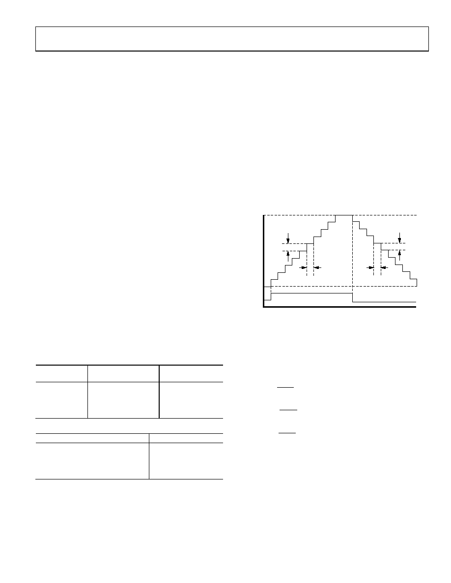
sweeping down toward S0. Figure 36 displays a linear sweep up
and then down using a profile pin. Note that the linear sweep
no-dwell bit is disabled; otherwise, the sweep accumulator
returns to 0 upon reaching E0.
05
24
6-
0
20
(F
RE
Q
UE
NCY
/P
HAS
E
/AM
P
L
IT
UDE
)
L
IN
EA
R
SW
EE
P
RDW
RSRR
FSRR
Δf,p,a
FDW
TIME
S0
E0
PROFILE PIN
Δf,p,a
Δt
Figure 36. Linear Sweep Parameters
For a piecemeal or a nonlinear transition between S0 and E0,
the delta-tuning words and ramp rate words can be repro-
grammed during the transition to produce the desired response.
The formulas for calculating the step size of RDW or FDW for
delta frequency, delta phase, or delta amplitude are as follows:
SYSCLK
RDW
f
×
=
Δ
32
2
(Hz)
°
×
=
360
2
14
RDW
ΔΦ
1024
2
10
×
=
Δ
RDW
a
(DAC full-scale current)
The formula for calculating delta time from RSRR or FSRR is
(
)
CLK
SYNC
RSRR
t
_
/
1
×
=
At 500 MSPS operation (SYNC_CLK = 125 MHz), the maxi-
mum time interval between steps is 1/125 MHz × 256 = 2.048 μs.
The minimum time interval is (1/125 MHz) × 1 = 8.0 ns.
The sweep ramp rate block (timer) consists of a loadable 8-bit
down counter that continuously counts down from the loaded
value to 1. When the ramp rate timer equals 1, the proper ramp rate
value is loaded and the counter begins counting down to 1 again.
相关PDF资料 |
PDF描述 |
|---|---|
| VE-2WT-IY-F2 | CONVERTER MOD DC/DC 6.5V 50W |
| VE-2WR-IY-F4 | CONVERTER MOD DC/DC 7.5V 50W |
| VE-2WR-IY-F1 | CONVERTER MOD DC/DC 7.5V 50W |
| VE-2WP-IY-F3 | CONVERTER MOD DC/DC 13.8V 50W |
| VE-2WN-IY-F2 | CONVERTER MOD DC/DC 18.5V 50W |
相关代理商/技术参数 |
参数描述 |
|---|---|
| AD9959BCPZ1 | 制造商:AD 制造商全称:Analog Devices 功能描述:4-Channel, 500 MSPS DDS with 10-Bit DACs |
| AD9959BCPZ-REEL7 | 功能描述:IC DDS QUAD 10BIT DAC 56LFCSP RoHS:是 类别:集成电路 (IC) >> 接口 - 直接数字合成 (DDS) 系列:- 产品变化通告:Product Discontinuance 27/Oct/2011 标准包装:2,500 系列:- 分辨率(位):10 b 主 fclk:25MHz 调节字宽(位):32 b 电源电压:2.97 V ~ 5.5 V 工作温度:-40°C ~ 85°C 安装类型:表面贴装 封装/外壳:16-TSSOP(0.173",4.40mm 宽) 供应商设备封装:16-TSSOP 包装:带卷 (TR) |
| AD9959BCPZ-REEL71 | 制造商:AD 制造商全称:Analog Devices 功能描述:4-Channel, 500 MSPS DDS with 10-Bit DACs |
| AD995PCBZ | 制造商:AD 制造商全称:Analog Devices 功能描述:1 GSPS Quadrature Digital Upconverter w/18-Bit IQ Data Path and 14-Bit DAC |
| AD9960BSTZ | 功能描述:RFID应答器 MxFE for RFID Reader Transceiver RoHS:否 制造商:Murata 存储容量:512 bit 工作温度范围:- 40 C to + 85 C 安装风格:SMD/SMT 封装 / 箱体: 封装:Reel |
发布紧急采购,3分钟左右您将得到回复。