- 您现在的位置:买卖IC网 > PDF目录10979 > AD9959BCPZ (Analog Devices Inc)IC DDS QUAD 10BIT DAC 56LFCSP PDF资料下载
参数资料
| 型号: | AD9959BCPZ |
| 厂商: | Analog Devices Inc |
| 文件页数: | 14/44页 |
| 文件大小: | 0K |
| 描述: | IC DDS QUAD 10BIT DAC 56LFCSP |
| 产品培训模块: | Direct Digital Synthesis Tutorial Series (1 of 7): Introduction Direct Digital Synthesizer Tutorial Series (7 of 7): DDS in Action Direct Digital Synthesis Tutorial Series (3 of 7): Angle to Amplitude Converter Direct Digital Synthesis Tutorial Series (6 of 7): SINC Envelope Correction Direct Digital Synthesis Tutorial Series (4 of 7): Digital-to-Analog Converter Direct Digital Synthesis Tutorial Series (2 of 7): The Accumulator |
| 设计资源: | Phase Coherent FSK Modulator (CN0186) |
| 标准包装: | 1 |
| 分辨率(位): | 10 b |
| 主 fclk: | 500MHz |
| 调节字宽(位): | 32 b |
| 电源电压: | 1.71 V ~ 1.96 V |
| 工作温度: | -40°C ~ 85°C |
| 安装类型: | 表面贴装 |
| 封装/外壳: | 56-VFQFN 裸露焊盘,CSP |
| 供应商设备封装: | 56-LFCSP-VQ(8x8) |
| 包装: | 托盘 |
| 产品目录页面: | 552 (CN2011-ZH PDF) |
第1页第2页第3页第4页第5页第6页第7页第8页第9页第10页第11页第12页第13页当前第14页第15页第16页第17页第18页第19页第20页第21页第22页第23页第24页第25页第26页第27页第28页第29页第30页第31页第32页第33页第34页第35页第36页第37页第38页第39页第40页第41页第42页第43页第44页
AD9959
Rev. B | Page 21 of 44
05
24
6-
01
9
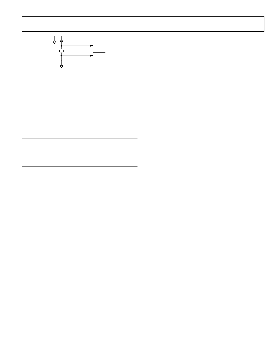
REF_CLK
PIN 23
25MHz
XTAL
REF_CLK
PIN 22
39pF
Figure 35.Crystal Input Configuration
SCALABLE DAC REFERENCE CURRENT CONTROL
MODE
RSET is common to all four DACs. As a result, the full-scale
currents are equal by default. The scalable DAC reference can
be used to set the full-scale current of each DAC independent
from one another. This is accomplished by using the register
bits CFR[9:8]. Table 5 shows how each DAC can be individually
scaled for independent channel control. This scaling provides
for binary attenuation.
Table 5. DAC Full-Scale Current Control
CFR[9:8]
LSB Current State
11
Full scale
01
Half scale
10
Quarter scale
00
Eighth scale
POWER-DOWN FUNCTIONS
The AD9959 supports an externally controlled power-down
feature and the more common software programmable power-
down bits found in previous Analog Devices DDS products.
The software control power-down allows the input clock circui-
try, the DAC, and the digital logic (for each separate channel) to
be individually powered down via unique control bits (CFR[7:6]).
These bits are not active when the externally controlled power-
down pin (PWR_DWN_CTL) is high. When the input pin,
PWR_DWN_CTL, is high, the AD9959 enters a power-down
mode based on the FR1[6] bit. When the PWR_DWN_CTL
input pin is low, the external power-down control is inactive.
When FR1[6] = 0 and the PWR_DWN_CTL input pin is high,
the AD9959 is put into a fast recovery power-down mode. In
this mode, the digital logic and the DAC digital logic are powered
down. The DAC bias circuitry, PLL, oscillator, and clock input
circuitry are not powered down.
When FR1[6] = 1 and the PWR_DWN_CTL input pin is high,
the AD9959 is put into full power-down mode. In this mode, all
functions are powered down. This includes the DAC and PLL,
which take a significant amount of time to power up. When the
PLL is bypassed, the PLL is shut down to conserve power.
When the PWR_DWN_CTL input pin is high, the individual
power-down bits (CFR[7:6] and FR1[7]) are invalid (don’t care)
and unused. When the PWR_DWN_CTL input pin is low, the
individual power-down bits control the power-down modes of
operation.
Note that the power-down signals are all designed such that
Logic 1 indicates the low power mode and Logic 0 indicates the
powered-up mode.
MODULATION MODE
The AD9959 can perform 2-/4-/8-/16-level modulation of
frequency, phase, or amplitude. Modulation is achieved by
applying data to the profile pins. Each channel can be program-
med separately, but the ability to modulate multiple channels
simultaneously is constrained by the limited number of profile
pins. For instance, 16-level modulation uses all four profile pins,
which inhibits modulation for three channels.
In addition, the AD9959 has the ability to ramp up or ramp
down the output amplitude before, during, or after a modulation
(FSK, PSK only) sequence. This is performed by using the 10-bit
output scalar. If the RU/RD feature is desired, unused profile
pins or unused SDIO_1/SDIO_2/SDIO_3 pins can be confi-
gured to initiate the operation. See the Output Amplitude
Control Mode section for more details of the RU/RD feature.
In modulation mode, each channel has its own set of control
bits to determine the type (frequency, phase, or amplitude)
of modulation. Each channel has 16 profile (channel word)
registers for flexibility. Register 0x0A through Register 0x18
are profile registers for modulation of frequency, phase, or
amplitude. Register 0x04, Register 0x05, and Register 0x06
are dedicated registers for frequency, phase, and amplitude,
respectively. These registers contain the first frequency, phase
offset, and amplitude word.
Frequency modulation has 32-bit resolution, phase modulation is
14 bits, and amplitude is 10 bits. When modulating phase or
amplitude, the word value must be MSB aligned in the profile
(channel word) registers and the unused bits are don’t care bits.
相关PDF资料 |
PDF描述 |
|---|---|
| VE-2WT-IY-F2 | CONVERTER MOD DC/DC 6.5V 50W |
| VE-2WR-IY-F4 | CONVERTER MOD DC/DC 7.5V 50W |
| VE-2WR-IY-F1 | CONVERTER MOD DC/DC 7.5V 50W |
| VE-2WP-IY-F3 | CONVERTER MOD DC/DC 13.8V 50W |
| VE-2WN-IY-F2 | CONVERTER MOD DC/DC 18.5V 50W |
相关代理商/技术参数 |
参数描述 |
|---|---|
| AD9959BCPZ1 | 制造商:AD 制造商全称:Analog Devices 功能描述:4-Channel, 500 MSPS DDS with 10-Bit DACs |
| AD9959BCPZ-REEL7 | 功能描述:IC DDS QUAD 10BIT DAC 56LFCSP RoHS:是 类别:集成电路 (IC) >> 接口 - 直接数字合成 (DDS) 系列:- 产品变化通告:Product Discontinuance 27/Oct/2011 标准包装:2,500 系列:- 分辨率(位):10 b 主 fclk:25MHz 调节字宽(位):32 b 电源电压:2.97 V ~ 5.5 V 工作温度:-40°C ~ 85°C 安装类型:表面贴装 封装/外壳:16-TSSOP(0.173",4.40mm 宽) 供应商设备封装:16-TSSOP 包装:带卷 (TR) |
| AD9959BCPZ-REEL71 | 制造商:AD 制造商全称:Analog Devices 功能描述:4-Channel, 500 MSPS DDS with 10-Bit DACs |
| AD995PCBZ | 制造商:AD 制造商全称:Analog Devices 功能描述:1 GSPS Quadrature Digital Upconverter w/18-Bit IQ Data Path and 14-Bit DAC |
| AD9960BSTZ | 功能描述:RFID应答器 MxFE for RFID Reader Transceiver RoHS:否 制造商:Murata 存储容量:512 bit 工作温度范围:- 40 C to + 85 C 安装风格:SMD/SMT 封装 / 箱体: 封装:Reel |
发布紧急采购,3分钟左右您将得到回复。