- 您现在的位置:买卖IC网 > PDF目录11674 > AD9979BCPZ (Analog Devices Inc)IC PROCESSOR CCD 14BIT 48-LFCSP PDF资料下载
参数资料
| 型号: | AD9979BCPZ |
| 厂商: | Analog Devices Inc |
| 文件页数: | 19/56页 |
| 文件大小: | 0K |
| 描述: | IC PROCESSOR CCD 14BIT 48-LFCSP |
| 标准包装: | 1 |
| 类型: | CCD 信号处理器,14 位 |
| 输入类型: | 逻辑 |
| 输出类型: | 逻辑 |
| 接口: | 3 线串口 |
| 电流 - 电源: | 48mA |
| 安装类型: | 表面贴装 |
| 封装/外壳: | 48-VFQFN 裸露焊盘,CSP |
| 供应商设备封装: | 48-LFCSP-VQ(7x7) |
| 包装: | 托盘 |
第1页第2页第3页第4页第5页第6页第7页第8页第9页第10页第11页第12页第13页第14页第15页第16页第17页第18页当前第19页第20页第21页第22页第23页第24页第25页第26页第27页第28页第29页第30页第31页第32页第33页第34页第35页第36页第37页第38页第39页第40页第41页第42页第43页第44页第45页第46页第47页第48页第49页第50页第51页第52页第53页第54页第55页第56页
AD9979
Rev. C | Page 26 of 56
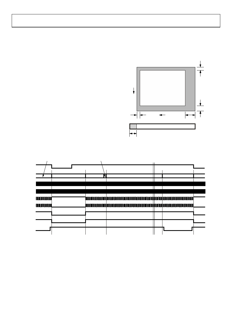
HORIZONTAL TIMING SEQUENCE EXAMPLE
Figure 34 shows an example of a CCD layout. The horizontal
register contains 28 dummy pixels, which occur on each line
clocked from the CCD. In the vertical direction, there are 10 optical
black (OB) lines at the front of the readout and 2 OB lines at the
back of the readout. The horizontal direction has 4 OB pixels in
the front and 48 in the back.
Figure 35 shows the basic sequence layout to use during the
effective pixel readout. The 48 OB pixels at the end of each line
are used for the CLPOB signals. PBLK is optional and is often
used to blank the digital outputs during the HBLK time. HBLK
is used during the vertical shift interval.
Because PBLK is used to isolate the CDS input (see the Analog
Front-End Description and Operation section), the PBLK signal
cannot be used during CLPOB operation. The change in the
offset behavior that occurs during PBLK impacts the accuracy
of the CLPOB circuitry.
The HBLK, CLPOB, and PBLK parameters are programmed in
the V-sequence registers. More elaborate clamping schemes can
be used, such as adding in a separate sequence to clamp in the
entire shield OB lines. This requires configuring a separate
V-sequence for clocking out the OB lines.
The CLPOB mask registers are also useful for disabling the
CLPOB on a few lines without affecting the setup of the
clamping sequences. It is important to use CLPOB only during
valid OB pixels. During other portions on the frame timing, such
as during vertical blanking or SG line timing, the CCD does not
output valid OB pixels. Any CLPOB pulses that occur during this
time cause errors in clamping operation, and therefore, cause
changes in the black level of the image.
HORIZONTAL CCD REGISTER
EFFECTIVE IMAGE AREA
28 DUMMY PIXELS
48 OB PIXELS
4 OB PIXELS
10 VERTICAL
OB LINES
2 VERTICAL
OB LINES
V
H
05
95
7-
0
36
Figure 34. Example CCD Configuration
VERTICAL SHIFT
VERT. SHIFT
CCD OUTPUT
SHP
SHD
H1/H3
H2/H4
HBLK
PBLK
CLPOB
OB
DUMMY
EFFECTIVE PIXELS
OB
HD
NOTES
1. IT IS RECOMMENDED THAT PBLK ACTIVE (LOW) NOT BE USED DURING CLPOB ACTIVE (LOW).
0
59
57
-0
37
Figure 35. Horizontal Sequence Example
相关PDF资料 |
PDF描述 |
|---|---|
| AD694BRZ | IC TRANSMITTER 4-20MA 16-SOIC |
| LTK001ACN8#PBF | IC THERMOCOUPL COMP& KIT 8DIP |
| AD693AQ | IC TRANSMITTER 4-20MA 20-CDIP |
| VE-J3K-IY-F3 | CONVERTER MOD DC/DC 40V 50W |
| AD9845BJSTZ | IC CCD SIGNAL PROC 12BIT 48-LQFP |
相关代理商/技术参数 |
参数描述 |
|---|---|
| AD9979BCPZRL | 功能描述:IC PROCESSOR CCD 14BIT 48-LFCSP RoHS:是 类别:集成电路 (IC) >> 接口 - 传感器和探测器接口 系列:- 其它有关文件:Automotive Product Guide 产品培训模块:Lead (SnPb) Finish for COTS Obsolescence Mitigation Program 标准包装:74 系列:- 类型:触控式传感器 输入类型:数字 输出类型:数字 接口:JTAG,串行 电流 - 电源:100µA 安装类型:表面贴装 封装/外壳:20-TSSOP(0.173",4.40mm 宽) 供应商设备封装:20-TSSOP 包装:管件 |
| AD9980 | 制造商:AD 制造商全称:Analog Devices 功能描述:High Performance 8-Bit Display Interface |
| AD9980/PCBZ | 功能描述:KIT EVALUATION AD9980 RoHS:是 类别:编程器,开发系统 >> 评估演示板和套件 系列:Advantiv® 标准包装:1 系列:PCI Express® (PCIe) 主要目的:接口,收发器,PCI Express 嵌入式:- 已用 IC / 零件:DS80PCI800 主要属性:- 次要属性:- 已供物品:板 |
| AD9980KSTZ-80 | 功能描述:IC INTERFACE 8BIT ANALOG 80LQFP RoHS:是 类别:集成电路 (IC) >> 接口 - 专用 系列:- 特色产品:NXP - I2C Interface 标准包装:1 系列:- 应用:2 通道 I²C 多路复用器 接口:I²C,SM 总线 电源电压:2.3 V ~ 5.5 V 封装/外壳:16-TSSOP(0.173",4.40mm 宽) 供应商设备封装:16-TSSOP 包装:剪切带 (CT) 安装类型:表面贴装 产品目录页面:825 (CN2011-ZH PDF) 其它名称:568-1854-1 |
| AD9980KSTZ-95 | 功能描述:IC INTERFACE 8BIT ANALOG 80LQFP RoHS:是 类别:集成电路 (IC) >> 接口 - 专用 系列:- 特色产品:NXP - I2C Interface 标准包装:1 系列:- 应用:2 通道 I²C 多路复用器 接口:I²C,SM 总线 电源电压:2.3 V ~ 5.5 V 封装/外壳:16-TSSOP(0.173",4.40mm 宽) 供应商设备封装:16-TSSOP 包装:剪切带 (CT) 安装类型:表面贴装 产品目录页面:825 (CN2011-ZH PDF) 其它名称:568-1854-1 |
发布紧急采购,3分钟左右您将得到回复。