- 您现在的位置:买卖IC网 > PDF目录11674 > AD9979BCPZ (Analog Devices Inc)IC PROCESSOR CCD 14BIT 48-LFCSP PDF资料下载
参数资料
| 型号: | AD9979BCPZ |
| 厂商: | Analog Devices Inc |
| 文件页数: | 7/56页 |
| 文件大小: | 0K |
| 描述: | IC PROCESSOR CCD 14BIT 48-LFCSP |
| 标准包装: | 1 |
| 类型: | CCD 信号处理器,14 位 |
| 输入类型: | 逻辑 |
| 输出类型: | 逻辑 |
| 接口: | 3 线串口 |
| 电流 - 电源: | 48mA |
| 安装类型: | 表面贴装 |
| 封装/外壳: | 48-VFQFN 裸露焊盘,CSP |
| 供应商设备封装: | 48-LFCSP-VQ(7x7) |
| 包装: | 托盘 |
第1页第2页第3页第4页第5页第6页当前第7页第8页第9页第10页第11页第12页第13页第14页第15页第16页第17页第18页第19页第20页第21页第22页第23页第24页第25页第26页第27页第28页第29页第30页第31页第32页第33页第34页第35页第36页第37页第38页第39页第40页第41页第42页第43页第44页第45页第46页第47页第48页第49页第50页第51页第52页第53页第54页第55页第56页
AD9979
Rev. C | Page 15 of 56
Table 8. HCLK Modes (Selected by Register Address 0x23, Bits[7:5])
HCLK Mode
Register Value
Description
Mode 1
001
H1 edges are programmable; H3 = H1, H2 = H4 = inverse of H1.
Mode 2
010
H1 edges are programmable; H3 = H1.
H2 edges are programmable; H4 = H2.
Mode 3
100
H1 edges are programmable; H2 = inverse of H1.
H3 edges are programmable; H4 = inverse of H3.
Invalid Selection
000, 011, 101, 110, 111
Invalid register settings.
Table 9. Horizontal Clock, RG, Drive, and Sample Control Registers Parameters
Name
Length
Range
Description
Polarity
1 bit
High/low
Polarity control for H1/H3 and RG; 0 = no inversion, 1 = inversion
Positive Edge
6 bits
0 to 63 edge location
Positive edge location for H1/H3 and RG
Negative Edge
6 bits
0 to 63 edge location
Negative edge location for H1/H3 and RG
Sample Location
6 bits
0 to 63 sample location
Sampling location for SHP and SHD
Drive Control
3 bits
0 to 7 current steps
Drive current for H1 to H4 and RG outputs (4.3 mA steps)
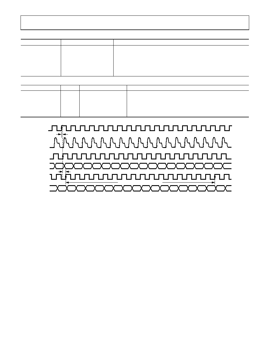
NOTES
1. EXAMPLE SHOWN FOR SHDLOC = 0.
2. HIGHER VALUES OF SHD AND/OR DOUTPHASE SHIFT DOUT TRANSITION TO THE RIGHT, WITH RESPECT TO CLI LOCATION.
DOUTPHASE
CLK
DOUT
CCDIN
CLI
SHD
(INTERNAL)
ADC OUT
(INTERNAL)
NN+2
N+1
N+3
N+13
N+12
N+11
N+10
N+9
N+7
N+6
N+5
N+4
N+14
SAMPLE PIXEL N
N+16
N+17
N+15
N–14
N–4
N–5
N–6
N–7
N–8
N–10
N–11
N–12
N–13
N–3
N–2
N–1
N
N+1
N–15
N–16
N–17
tCLIDLY
N–4
N–5
N–6
N–7
N–8
N–3
N–2
N–1
N
N+1
tDOUTINH
PIPELINE LATENCY = 16 CYCLES
N–9
N–14
N–10
N–11
N–12
N–13
N–15
N–16
N–17
N–9
N+8
05
95
7-
0
22
Figure 20. Pipeline Delay of AFE Data Outputs
H-Driver and RG Outputs
In addition to the programmable timing positions, the AD9979
features on-chip output drivers for the HL, RG, and H1 to H4
outputs. These drivers are powerful enough to directly drive
the CCD inputs. The H-driver and RG-driver currents can be
adjusted for optimum rise/fall times into a particular load by
using the drive strength control register (Address 0x35). Use
the register to adjust the drive strength in 4.3 mA increments.
The minimum setting of 0 is equal to off or three-state, and the
maximum setting of 7 is equal to 30.1 mA.
Digital Data Outputs
For maximum system flexibility, the AD9979 uses DOUTPHASEN
and DOUTPHASEP (Address 0x37, Bits[11:0]) to select the
location for the start of each new pixel data value. Any edge
location from 0 to 63 can be programmed. Register 0x37
determines the start location of the data output and the
DOUTPHASEx clock rising edge with respect to the master
clock input CLI.
The pipeline delay through the AD9979 is shown in Figure 20.
After the CCD input is sampled by SHD, there is a 16-cycle
delay before the data is available.
相关PDF资料 |
PDF描述 |
|---|---|
| AD694BRZ | IC TRANSMITTER 4-20MA 16-SOIC |
| LTK001ACN8#PBF | IC THERMOCOUPL COMP& KIT 8DIP |
| AD693AQ | IC TRANSMITTER 4-20MA 20-CDIP |
| VE-J3K-IY-F3 | CONVERTER MOD DC/DC 40V 50W |
| AD9845BJSTZ | IC CCD SIGNAL PROC 12BIT 48-LQFP |
相关代理商/技术参数 |
参数描述 |
|---|---|
| AD9979BCPZRL | 功能描述:IC PROCESSOR CCD 14BIT 48-LFCSP RoHS:是 类别:集成电路 (IC) >> 接口 - 传感器和探测器接口 系列:- 其它有关文件:Automotive Product Guide 产品培训模块:Lead (SnPb) Finish for COTS Obsolescence Mitigation Program 标准包装:74 系列:- 类型:触控式传感器 输入类型:数字 输出类型:数字 接口:JTAG,串行 电流 - 电源:100µA 安装类型:表面贴装 封装/外壳:20-TSSOP(0.173",4.40mm 宽) 供应商设备封装:20-TSSOP 包装:管件 |
| AD9980 | 制造商:AD 制造商全称:Analog Devices 功能描述:High Performance 8-Bit Display Interface |
| AD9980/PCBZ | 功能描述:KIT EVALUATION AD9980 RoHS:是 类别:编程器,开发系统 >> 评估演示板和套件 系列:Advantiv® 标准包装:1 系列:PCI Express® (PCIe) 主要目的:接口,收发器,PCI Express 嵌入式:- 已用 IC / 零件:DS80PCI800 主要属性:- 次要属性:- 已供物品:板 |
| AD9980KSTZ-80 | 功能描述:IC INTERFACE 8BIT ANALOG 80LQFP RoHS:是 类别:集成电路 (IC) >> 接口 - 专用 系列:- 特色产品:NXP - I2C Interface 标准包装:1 系列:- 应用:2 通道 I²C 多路复用器 接口:I²C,SM 总线 电源电压:2.3 V ~ 5.5 V 封装/外壳:16-TSSOP(0.173",4.40mm 宽) 供应商设备封装:16-TSSOP 包装:剪切带 (CT) 安装类型:表面贴装 产品目录页面:825 (CN2011-ZH PDF) 其它名称:568-1854-1 |
| AD9980KSTZ-95 | 功能描述:IC INTERFACE 8BIT ANALOG 80LQFP RoHS:是 类别:集成电路 (IC) >> 接口 - 专用 系列:- 特色产品:NXP - I2C Interface 标准包装:1 系列:- 应用:2 通道 I²C 多路复用器 接口:I²C,SM 总线 电源电压:2.3 V ~ 5.5 V 封装/外壳:16-TSSOP(0.173",4.40mm 宽) 供应商设备封装:16-TSSOP 包装:剪切带 (CT) 安装类型:表面贴装 产品目录页面:825 (CN2011-ZH PDF) 其它名称:568-1854-1 |
发布紧急采购,3分钟左右您将得到回复。