- 您现在的位置:买卖IC网 > PDF目录11659 > AD9991KCPZ (Analog Devices Inc)IC CCD SIGNAL PROCESSOR 56-LFCSP PDF资料下载
参数资料
| 型号: | AD9991KCPZ |
| 厂商: | Analog Devices Inc |
| 文件页数: | 15/60页 |
| 文件大小: | 0K |
| 描述: | IC CCD SIGNAL PROCESSOR 56-LFCSP |
| 标准包装: | 1 |
| 类型: | CCD 信号处理器,10 位 |
| 输入类型: | 逻辑 |
| 输出类型: | 逻辑 |
| 接口: | 3 线串口 |
| 安装类型: | 表面贴装 |
| 封装/外壳: | 56-VFQFN 裸露焊盘,CSP |
| 供应商设备封装: | 56-LFCSP-VQ(8x8) |
| 包装: | 带卷 (TR) |
第1页第2页第3页第4页第5页第6页第7页第8页第9页第10页第11页第12页第13页第14页当前第15页第16页第17页第18页第19页第20页第21页第22页第23页第24页第25页第26页第27页第28页第29页第30页第31页第32页第33页第34页第35页第36页第37页第38页第39页第40页第41页第42页第43页第44页第45页第46页第47页第48页第49页第50页第51页第52页第53页第54页第55页第56页第57页第58页第59页第60页
AD9991
–22–
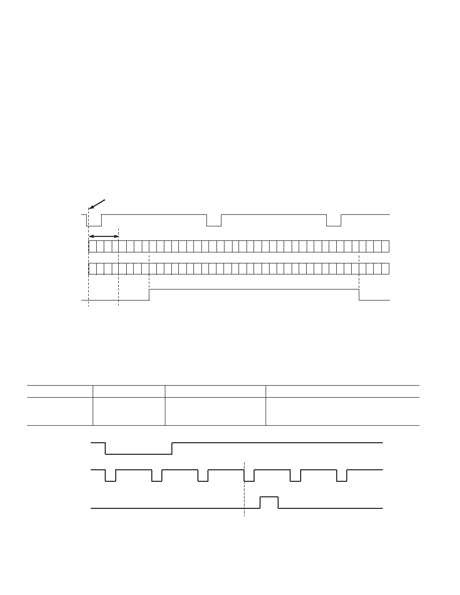
The example shown in Figure 22 illustrates this operation. The
rst toggle position is 2, and the second toggle position is 9. In
non-Multiplier mode, this would cause the V-sequence to toggle
at pixel 2 and then pixel 9 within a single HD line. However,
toggle positions are now multiplied by the VTPLEN = 4, so the
rst toggle occurs at pixel count 8, and the second toggle occurs
at pixel count 36. Sweep mode has also been enabled to allow the
toggle positions to cross the HD line boundaries.
Vertical Sensor Gate (Shift Gate) Patterns
In an Interline CCD, the vertical sensor gates (VSG) are used
to transfer the pixel charges from the light-sensitive image area
into light-shielded vertical registers. From the light-shield verti-
cal registers, the image is then read out line-by-line by using the
vertical transfer pulses V1–V6 in conjunction with the high speed
horizontal clocks.
Table IX contains the summary of the VSG pattern registers. The
AD9991 has ve VSG outputs, VSG1–VSG5. Each of the out-
puts can be assigned to one of four programmed patterns by using
the SGPATSEL registers. Each pattern is generated in a similar
manner as the V-pattern groups, with a programmable start polar-
ity (SGPOL), rst toggle position (SGTOG1), and second toggle
position (SGTOG2). The active line where the VSG1–VSG5
pulses occur is programmable using the SGLINE1 and SGLINE2
registers. Additionally, any of the VSG1–VSG5 pulses may be
individually disabled by using the SGMASK register. The individ-
ual masking allows all of the SG patterns to be preprogrammed,
and the appropriate pulses for the different elds can be separately
enabled. For maximum exibility, the SGPATSEL, SGMASK,
and SGLINE registers are separately programmable for each eld.
More detail is given in the Complete Field section.
V1–V6
HD
VPATLEN
MULTIPLIER MODE V-PATTERN GROUP PROPERTIES:
1. START POLARITY (ABOVE: STARTPOL = 0)
2. FIRST, SECOND, AND THIRD TOGGLE POSITIONS (ABOVE: VTOG1 = 2, VTOG2 = 9)
3. LENGTH OF VPAT COUNTER (ABOVE: VPATLEN = 4). THIS IS THE MINIMUM RESOLUTION FOR TOGGLE POSITION CHANGES.
4. TOGGLE POSITIONS OCCUR AT LOCATION EQUAL TO (VTOG
VPATLEN)
5. IF SWEEP REGION IS ENABLED, THE V-PULSES MAY ALSO CROSS THE HD BOUNDRIES, AS SHOWN ABOVE
12
34
123412341234123412341234
1
2
34
1
2
3
4
1
2
34
START POSITION OF VPAT GROUP IS STILL PROGRAMMED IN THE V-SEQUENCE REGISTERS
PIXEL
NUMBER
1
234
5678
9 10 11 12 13 14 15 16 17 18 19 20 21 22 23 24 25 26 27 28 29 30 31 32 33 34 35 36 37 38 39 40
3
55
4
1
2
4
2
Figure 22. Example of Multiplier Region for Wide Vertical Pulse Timing
Table IX. VSG Pattern Registers (also see Field Registers in Table VII)
Register
Length
Range
Description
SGPOL
1b
High/Low
Sensor Gate Starting Polarity for SG Pattern 0–3
SGTOG1
12b
0–4095 Pixel Location
First Toggle Position for SG Pattern 0–3
SGTOG2
12b
0–4095 Pixel Location
Second Toggle Position for SG Pattern 0–3
VD
HD
PROGRAMMABLE SETTINGS FOR EACH PATTERN:
1. START POLARITY OF PULSE
2. FIRST TOGGLE POSITION
3. SECOND TOGGLE POSITION
4. ACTIVE LINE FOR VSG PULSES WITHIN THE FIELD (PROGRAMMABLE IN THE FIELD REGISTER, NOT FOR EACH PATTERN)
VSG PATTERNS
4
12
3
Figure 23. Vertical Sensor Gate Pulse Placement
REV. 0
相关PDF资料 |
PDF描述 |
|---|---|
| VE-JN4-IZ-B1 | CONVERTER MOD DC/DC 48V 25W |
| VE-JN4-IY-F4 | CONVERTER MOD DC/DC 48V 50W |
| VE-JN4-IY-F2 | CONVERTER MOD DC/DC 48V 50W |
| AD9923ABBCZRL | IC PROCESSOR CCD 12BIT 105CSPBGA |
| 1-413589-1 | CONN PLUG BNC JIS 3C-2V CRIMP AU |
相关代理商/技术参数 |
参数描述 |
|---|---|
| AD9991KCPZRL | 功能描述:IC CCD SIGNAL PROCESSOR 56-LFCSP RoHS:是 类别:集成电路 (IC) >> 接口 - 传感器和探测器接口 系列:- 其它有关文件:Automotive Product Guide 产品培训模块:Lead (SnPb) Finish for COTS Obsolescence Mitigation Program 标准包装:74 系列:- 类型:触控式传感器 输入类型:数字 输出类型:数字 接口:JTAG,串行 电流 - 电源:100µA 安装类型:表面贴装 封装/外壳:20-TSSOP(0.173",4.40mm 宽) 供应商设备封装:20-TSSOP 包装:管件 |
| AD9992 | 制造商:AD 制造商全称:Analog Devices 功能描述:12-Bit CCD Signal Processor with Precision Timing Generator |
| AD9992_07 | 制造商:AD 制造商全称:Analog Devices 功能描述:12-Bit CCD Signal Processor with Precision Timing Generator |
| AD9992BBCZ | 功能描述:IC CCD SGNL PROC 12BIT 105CSPBGA RoHS:是 类别:集成电路 (IC) >> 接口 - 传感器和探测器接口 系列:- 其它有关文件:Automotive Product Guide 产品培训模块:Lead (SnPb) Finish for COTS Obsolescence Mitigation Program 标准包装:74 系列:- 类型:触控式传感器 输入类型:数字 输出类型:数字 接口:JTAG,串行 电流 - 电源:100µA 安装类型:表面贴装 封装/外壳:20-TSSOP(0.173",4.40mm 宽) 供应商设备封装:20-TSSOP 包装:管件 |
| AD9992BBCZRL | 功能描述:IC CCD SGNL PROC 12BIT 105CSPBGA RoHS:是 类别:集成电路 (IC) >> 接口 - 传感器和探测器接口 系列:- 其它有关文件:Automotive Product Guide 产品培训模块:Lead (SnPb) Finish for COTS Obsolescence Mitigation Program 标准包装:74 系列:- 类型:触控式传感器 输入类型:数字 输出类型:数字 接口:JTAG,串行 电流 - 电源:100µA 安装类型:表面贴装 封装/外壳:20-TSSOP(0.173",4.40mm 宽) 供应商设备封装:20-TSSOP 包装:管件 |
发布紧急采购,3分钟左右您将得到回复。