- 您现在的位置:买卖IC网 > PDF目录11659 > AD9923ABBCZRL (Analog Devices Inc)IC PROCESSOR CCD 12BIT 105CSPBGA PDF资料下载
参数资料
| 型号: | AD9923ABBCZRL |
| 厂商: | Analog Devices Inc |
| 文件页数: | 1/84页 |
| 文件大小: | 0K |
| 描述: | IC PROCESSOR CCD 12BIT 105CSPBGA |
| 标准包装: | 2,000 |
| 类型: | CCD 信号处理器,12 位 |
| 输入类型: | 逻辑 |
| 输出类型: | 逻辑 |
| 接口: | 3 线串口 |
| 电流 - 电源: | 20mA |
| 安装类型: | 表面贴装 |
| 封装/外壳: | 105-LFBGA,CSPBGA |
| 供应商设备封装: | 105-CSPBGA(8x8) |
| 包装: | 带卷 (TR) |
当前第1页第2页第3页第4页第5页第6页第7页第8页第9页第10页第11页第12页第13页第14页第15页第16页第17页第18页第19页第20页第21页第22页第23页第24页第25页第26页第27页第28页第29页第30页第31页第32页第33页第34页第35页第36页第37页第38页第39页第40页第41页第42页第43页第44页第45页第46页第47页第48页第49页第50页第51页第52页第53页第54页第55页第56页第57页第58页第59页第60页第61页第62页第63页第64页第65页第66页第67页第68页第69页第70页第71页第72页第73页第74页第75页第76页第77页第78页第79页第80页第81页第82页第83页第84页
CCD Signal Processor with V-Driver and
Precision Timing Generator
AD9923A
Rev. A
Information furnished by Analog Devices is believed to be accurate and reliable. However, no
responsibilityis assumedbyAnalogDevicesforitsuse,norforanyinfringementsof patentsorother
rightsofthirdpartiesthatmayresultfromitsuse.Specificationssubjecttochangewithoutnotice.No
license is granted by implication or otherwise under any patent or patent rights of Analog Devices.
Trademarksandregisteredtrademarksarethepropertyoftheirrespectiveowners.
One Technology Way, P.O. Box 9106, Norwood, MA 02062-9106, U.S.A.
Tel: 781.329.4700
www.analog.com
Fax: 781.461.3113
2006–2010 Analog Devices, Inc. All rights reserved.
FEATURES
Integrated 15-channel V-driver
12-bit, 36 MHz analog-to-digital converter (ADC)
Similar register map to the AD9923
5-field, 10-phase vertical clock support
Complete on-chip timing generator
Precision Timing core with <600 ps resolution
Correlated double sampler (CDS)
6 dB to 42 dB 10-bit variable gain amplifier (VGA)
Black level clamp with variable level control
On-chip 3 V horizontal and RG drivers
2-phase and 4-phase H-clock modes
Electronic and mechanical shutter support
On-chip driver for external crystal
On-chip sync generator with external sync input
8 mm × 8 mm CSP_BGA package with 0.65 mm pitch
APPLICATIONS
Digital still cameras
GENERAL DESCRIPTION
The AD9923A is a complete 36 MHz front-end solution for
digital still cameras and other CCD imaging applications.
Similar to the AD9923 product, the AD9923A includes the
analog front end (AFE), a fully programmable timing generator
(TG), and a 15-channel vertical driver (V-driver). A Precision
Timingcore allows adjustment of high speed clocks with
approximately 600 ps resolution at 36 MHz operation.
The on-chip V-driver supports up to 15 channels for use with
5-field, 10-phase CCDs.
The analog front end includes black level clamping, CDS, VGA,
and a 12-bit ADC. The timing generator and V-driver provide
all the necessary CCD clocks: RG, H-clocks, vertical clocks, sensor
gate pulses, substrate clock, and substrate bias control. The
internal registers are programmed using a 3-wire serial
interface.
Packaged in an 8 mm × 8 mm CSP_BGA, the AD9923A is
specified over an operating temperature range of 25°C to +85°C.
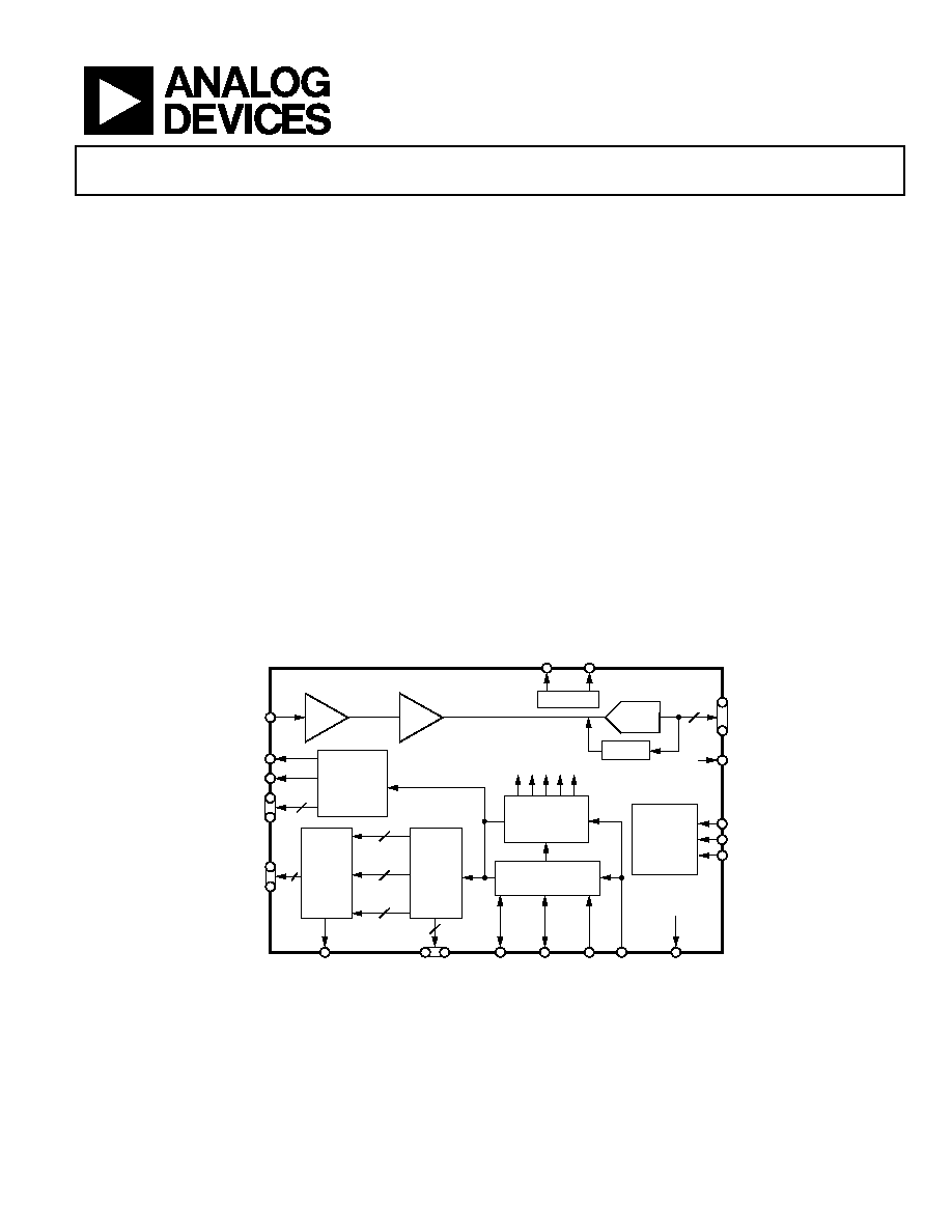
FUNCTIONAL BLOCK DIAGRAM
AD9923A
DCLK
CLAMP
D0 TO D11
CCDIN
12-BIT
ADC
–3dB, 0dB, +3dB, +6dB
CDS
12
REFT
REFB
VREF
+6dB TO +42dB
VGA
HORIZONTAL
DRIVERS
RG
HL
H1 TO H4
4
INTERNAL
REGISTERS
SL
SDI
SCK
SYNC
GENERATOR
PRECISION
TIMING
GENERATOR
INTERNAL CLOCKS
HD
VD
SYNC
CLI
CLO
VSUB, MSHUT,
STROBE
SUBCK
VERTICAL
TIMING
CONTROL
V-DRIVER
V1, V2, V3,
V4, V5A, V5B,
V6, V7A, V7B,
V8, V9, V10,
V11, V12, V13
15
3
XSUBCK,
XSUBCNT
2
XSG1 TO
XSG8
8
XV1 TO
XV13
13
05
58
6-
0
01
Figure 1.
相关PDF资料 |
PDF描述 |
|---|---|
| 1-413589-1 | CONN PLUG BNC JIS 3C-2V CRIMP AU |
| 8-5227079-1 | CONN PLUG BNC CRIMP DUAL |
| 2081204-1 | CONN JACK SMA BULKHEAD RG402 |
| MS3102R36-18S | CONN RCPT 31POS BOX MNT W/SCKT |
| AD8497CRMZ-R7 | IC THERMOCOUPLE A W/COMP 8MSOP |
相关代理商/技术参数 |
参数描述 |
|---|---|
| AD9923BBCZ | 制造商:Rochester Electronics LLC 功能描述:- Bulk 制造商:Analog Devices 功能描述: |
| AD9923BBCZRL | 制造商:Rochester Electronics LLC 功能描述: 制造商:Analog Devices 功能描述: |
| AD9924BBCZ | 制造商:Analog Devices 功能描述: |
| AD9924BBCZRL | 制造商:Rochester Electronics LLC 功能描述:- Bulk |
| AD9925 | 制造商:AD 制造商全称:Analog Devices 功能描述:CCD Signal Processor with Vertical Driver and Precision Timing Generator |
发布紧急采购,3分钟左右您将得到回复。