- 您现在的位置:买卖IC网 > PDF目录11659 > AD9923ABBCZRL (Analog Devices Inc)IC PROCESSOR CCD 12BIT 105CSPBGA PDF资料下载
参数资料
| 型号: | AD9923ABBCZRL |
| 厂商: | Analog Devices Inc |
| 文件页数: | 51/84页 |
| 文件大小: | 0K |
| 描述: | IC PROCESSOR CCD 12BIT 105CSPBGA |
| 标准包装: | 2,000 |
| 类型: | CCD 信号处理器,12 位 |
| 输入类型: | 逻辑 |
| 输出类型: | 逻辑 |
| 接口: | 3 线串口 |
| 电流 - 电源: | 20mA |
| 安装类型: | 表面贴装 |
| 封装/外壳: | 105-LFBGA,CSPBGA |
| 供应商设备封装: | 105-CSPBGA(8x8) |
| 包装: | 带卷 (TR) |
第1页第2页第3页第4页第5页第6页第7页第8页第9页第10页第11页第12页第13页第14页第15页第16页第17页第18页第19页第20页第21页第22页第23页第24页第25页第26页第27页第28页第29页第30页第31页第32页第33页第34页第35页第36页第37页第38页第39页第40页第41页第42页第43页第44页第45页第46页第47页第48页第49页第50页当前第51页第52页第53页第54页第55页第56页第57页第58页第59页第60页第61页第62页第63页第64页第65页第66页第67页第68页第69页第70页第71页第72页第73页第74页第75页第76页第77页第78页第79页第80页第81页第82页第83页第84页
AD9923A
Rev. A | Page 55 of 84
6dB ~ 42dB
CCDIN
CLI
DIGITAL
FILTER
CLPOB
DC RESTORE
OPTICAL BLACK
CLAMP
12-BIT
ADC
VGA
DAC
8
CDS
INTERNAL
VREF
2V FULL SCALE
PRECISION
TIMING
GENERATION
SHP
SHD
1.5V
OUTPUT
DATA
LATCH
REFT
REFB
DOUT PHASE
V-H
TIMING
GENERATION
SHP SHD
DOUT
PHASE
CLPOB PBLK
PBLK
1.0V
2.0V
DOUT
DCLK
AD9923A
0.1F
VGA GAIN
REGISTER
0.1F 0.1F
CLAMP LEVEL
REGISTER
12
DOUT
DLY
DCLK
MODE
FIXED
DELAY
CLI
1
0
0
55
86
-0
71
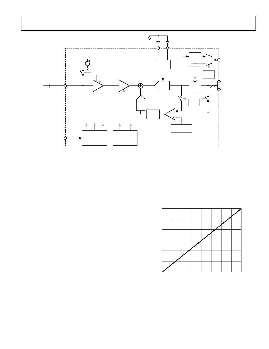
Figure 73. Analog Front End Functional Block Diagram
ANALOG FRONT END DESCRIPTION/OPERATION
The AD9923A signal processing chain is shown in Figure 73.
Each step is essential to achieve a high quality image from the
raw CCD pixel data.
DC Restore
To reduce the large dc offset of the CCD output signal, a dc restore
circuit is used with an external 0.1 μF series coupling capacitor.
This restores the dc level of the CCD signal to approximately 1.5 V
so that it is compatible with the 3 V supply voltage of the AD9923A.
Correlated Double Sampler
The CDS circuit samples each CCD pixel twice to extract video
information and reject low frequency noise. The timing shown in
Figure 20 illustrates how the two internally generated CDS
clocks, SHP and SHD, are used to sample the reference and data
levels of the CCD signal, respectively. The placement of the SHP
and SHD sampling edges is determined by the setting of the
SHPLOC and SHDLOC registers located at Address 0x37.
Placement of these clock signals is critical to achieve the best
CCD performance.
The CDS gain can be set to 3 dB, 0 dB (default), +3 dB, or +6 dB
in the CDSGAIN register, Address 0x04. The +3 dB and +6 dB
settings improve noise performance, but reduce the input range
(see Figure 8).
Variable Gain Amplifier
The VGA stage provides gain in the range of 6 dB to 42 dB,
programmable with 10-bit resolution through the serial digital
interface. A minimum gain of 6 dB is needed to match a 1 V input
signal with an ADC full-scale range of 2 V. When compared to 1 V
full-scale systems, the equivalent range of gain is 0 dB to 36 dB.
The VGA gain curve follows a linear-in-dB characteristic. The
exact VGA gain can be calculated for any gain register value
using the following equation
Gain (dB) = (0.0358 × Code) + 5.5 dB
where the code range is 0 to 1023.
0
55
86
-0
72
VGA GAIN REGISTER CODE
V
G
A
G
AI
N
(
d
B)
42
36
30
24
18
12
6
0
127
255
383
511
639
767
895
1023
Figure 74. VGA Gain Curve
ADC
The AD9923A uses a high performance ADC architecture
optimized for high speed and low power. Differential nonlin-
earity (DNL) performance is typically better than 1 LSB. The
typical linearity and noise performance plots.
相关PDF资料 |
PDF描述 |
|---|---|
| 1-413589-1 | CONN PLUG BNC JIS 3C-2V CRIMP AU |
| 8-5227079-1 | CONN PLUG BNC CRIMP DUAL |
| 2081204-1 | CONN JACK SMA BULKHEAD RG402 |
| MS3102R36-18S | CONN RCPT 31POS BOX MNT W/SCKT |
| AD8497CRMZ-R7 | IC THERMOCOUPLE A W/COMP 8MSOP |
相关代理商/技术参数 |
参数描述 |
|---|---|
| AD9923BBCZ | 制造商:Rochester Electronics LLC 功能描述:- Bulk 制造商:Analog Devices 功能描述: |
| AD9923BBCZRL | 制造商:Rochester Electronics LLC 功能描述: 制造商:Analog Devices 功能描述: |
| AD9924BBCZ | 制造商:Analog Devices 功能描述: |
| AD9924BBCZRL | 制造商:Rochester Electronics LLC 功能描述:- Bulk |
| AD9925 | 制造商:AD 制造商全称:Analog Devices 功能描述:CCD Signal Processor with Vertical Driver and Precision Timing Generator |
发布紧急采购,3分钟左右您将得到回复。