- 您现在的位置:买卖IC网 > PDF目录11659 > AD9923ABBCZRL (Analog Devices Inc)IC PROCESSOR CCD 12BIT 105CSPBGA PDF资料下载
参数资料
| 型号: | AD9923ABBCZRL |
| 厂商: | Analog Devices Inc |
| 文件页数: | 56/84页 |
| 文件大小: | 0K |
| 描述: | IC PROCESSOR CCD 12BIT 105CSPBGA |
| 标准包装: | 2,000 |
| 类型: | CCD 信号处理器,12 位 |
| 输入类型: | 逻辑 |
| 输出类型: | 逻辑 |
| 接口: | 3 线串口 |
| 电流 - 电源: | 20mA |
| 安装类型: | 表面贴装 |
| 封装/外壳: | 105-LFBGA,CSPBGA |
| 供应商设备封装: | 105-CSPBGA(8x8) |
| 包装: | 带卷 (TR) |
第1页第2页第3页第4页第5页第6页第7页第8页第9页第10页第11页第12页第13页第14页第15页第16页第17页第18页第19页第20页第21页第22页第23页第24页第25页第26页第27页第28页第29页第30页第31页第32页第33页第34页第35页第36页第37页第38页第39页第40页第41页第42页第43页第44页第45页第46页第47页第48页第49页第50页第51页第52页第53页第54页第55页当前第56页第57页第58页第59页第60页第61页第62页第63页第64页第65页第66页第67页第68页第69页第70页第71页第72页第73页第74页第75页第76页第77页第78页第79页第80页第81页第82页第83页第84页
AD9923A
Rev. A | Page 6 of 84
Parameter
Conditions/Comments
Min
Typ
Max
Unit
BLACK LEVEL CLAMP
Measured at ADC output
Clamp Level Resolution
1024
Steps
Minimum Clamp Level (Code 0)
0
LSB
Maximum Clamp Level (Code 1023)
255
LSB
ANALOG-TO-DIGITAL CONVERTER (ADC)
Resolution
12
Bits
Differential Nonlinearity (DNL)
1.0
±0.5
+1.0
LSB
No Missing Codes
Guaranteed
Full-Scale Input Voltage
2.0
V
VOLTAGE REFERENCE
Reference Top Voltage (REFT)
2.0
V
Reference Bottom Voltage (REFB)
1.0
V
SYSTEM PERFORMANCE
Includes entire signal chain
Gain Accuracy
Low Gain (VGA Code 15)
Default CDS gain (0 dB)
6.0
6.5
7.0
dB
Maximum Gain (VGA Code 1023)
42.0
42.5
43.0
dB
Peak Nonlinearity, 500 mV Input Signal
12 dB gain applied
0.1
%
Total Output Noise
AC-grounded input, 6 dB gain applied
1.0
LSB rms
Power Supply Rejection (PSR)
Measured with step change on supply
50
dB
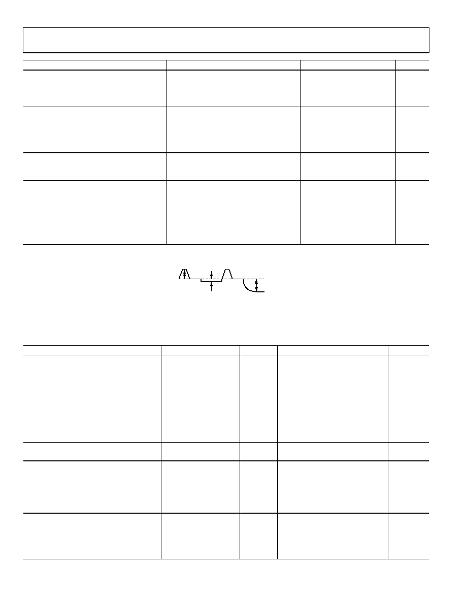
1 Input signal characteristics are defined as shown in Figure 3.
200mV MAX
OPTICAL BLACK PIXEL
500mV TYP
RESET TRANSIENT
1V MAX
INPUT SIGNAL RANGE
(0dB CDS GAIN)
05
58
6-
00
3
Figure 3. Signal Characteristics
TIMING SPECIFICATIONS
CL = 20 pF, AVDD = DVDD = DRVDD = 3.0 V, fCLI = 36 MHz, unless otherwise noted.
Table 6.
Parameter
Conditions/Comments
Symbol
Min
Typ
Max
Unit
MASTER CLOCK, CLI
CLI Clock Period
tCONV
27.8
ns
CLI High/Low Pulse Width
11.2
13.9
16.6
ns
Delay from CLI Rising Edge to Internal Pixel
Position 0
tCLIDLY
6
ns
AFE CLPOB Pulse Width1, 2
2
20
Pixels
Allowable Region for HD Falling Edge to CLI
Rising Edge
Only valid in slave mode
tHDCLI
4
tCONV 2
ns
SHP Inhibit Region
Only valid in slave mode
tSHPINH
30
39
Edge
location
AFE SAMPLE LOCATION1
SHP Sample Edge to SHD Sample Edge
tS1
11.6
13.9
ns
DATA OUTPUTS
Output Delay from DCLK Rising Edge1
tOD
8
ns
Inhibited Area for DOUTPHASE Edge
Location
SHD
SHD + 11
Edge
location
Pipeline Delay from SHP/SHD Sampling to
Data Output
16
Cycles
SERIAL INTERFACE
Maximum SCK Frequency
fSCLK
36
MHz
SL to SCK Setup Time
tLS
10
ns
SCK to SL Hold Time
tLH
10
ns
SDATA Valid to SCK Rising Edge Setup
tDS
10
ns
相关PDF资料 |
PDF描述 |
|---|---|
| 1-413589-1 | CONN PLUG BNC JIS 3C-2V CRIMP AU |
| 8-5227079-1 | CONN PLUG BNC CRIMP DUAL |
| 2081204-1 | CONN JACK SMA BULKHEAD RG402 |
| MS3102R36-18S | CONN RCPT 31POS BOX MNT W/SCKT |
| AD8497CRMZ-R7 | IC THERMOCOUPLE A W/COMP 8MSOP |
相关代理商/技术参数 |
参数描述 |
|---|---|
| AD9923BBCZ | 制造商:Rochester Electronics LLC 功能描述:- Bulk 制造商:Analog Devices 功能描述: |
| AD9923BBCZRL | 制造商:Rochester Electronics LLC 功能描述: 制造商:Analog Devices 功能描述: |
| AD9924BBCZ | 制造商:Analog Devices 功能描述: |
| AD9924BBCZRL | 制造商:Rochester Electronics LLC 功能描述:- Bulk |
| AD9925 | 制造商:AD 制造商全称:Analog Devices 功能描述:CCD Signal Processor with Vertical Driver and Precision Timing Generator |
发布紧急采购,3分钟左右您将得到回复。