- 您现在的位置:买卖IC网 > PDF目录1895 > AD9992BBCZRL (Analog Devices Inc)IC CCD SGNL PROC 12BIT 105CSPBGA PDF资料下载
参数资料
| 型号: | AD9992BBCZRL |
| 厂商: | Analog Devices Inc |
| 文件页数: | 7/92页 |
| 文件大小: | 0K |
| 描述: | IC CCD SGNL PROC 12BIT 105CSPBGA |
| 产品变化通告: | AD9992 Discontinuation 22/Feb/2012 |
| 标准包装: | 2,000 |
| 类型: | CCD 信号处理器,12 位 |
| 输入类型: | 逻辑 |
| 输出类型: | 逻辑 |
| 接口: | 3 线串口 |
| 电流 - 电源: | 27mA |
| 安装类型: | 表面贴装 |
| 封装/外壳: | 105-LFBGA,CSPBGA |
| 供应商设备封装: | 105-CSPBGA(8x8) |
| 包装: | 带卷 (TR) |
第1页第2页第3页第4页第5页第6页当前第7页第8页第9页第10页第11页第12页第13页第14页第15页第16页第17页第18页第19页第20页第21页第22页第23页第24页第25页第26页第27页第28页第29页第30页第31页第32页第33页第34页第35页第36页第37页第38页第39页第40页第41页第42页第43页第44页第45页第46页第47页第48页第49页第50页第51页第52页第53页第54页第55页第56页第57页第58页第59页第60页第61页第62页第63页第64页第65页第66页第67页第68页第69页第70页第71页第72页第73页第74页第75页第76页第77页第78页第79页第80页第81页第82页第83页第84页第85页第86页第87页第88页第89页第90页第91页第92页
AD9992
Rev. C | Page 15 of 92
HIGH SPEED PRECISION TIMING CORE
The AD9992 generates high speed timing signals using the flexible
Precision Timing core. This core is the foundation for generating
timing used for both the CCD and the AFE; it includes the reset
gate RG, horizontal drivers H1 to H8, HL, and SHP/SHD sample
clocks. A unique architecture makes it routine for the system
designer to optimize image quality by providing precise control
over the horizontal CCD readout and the AFE correlated
double sampling.
The high speed timing of the AD9992 operates the same way in
either master or slave mode configuration. For more informa-
tion on synchronization and pipeline delays, see the Power-Up
Sequence for Master Mode section.
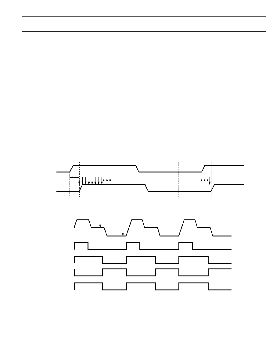
Timing Resolution
The Precision Timing core uses a 1× master clock input (CLI) as
a reference. This clock should be the same as the CCD pixel
clock frequency. Figure 15 illustrates how the internal timing
core divides the master clock period into 64 steps or edge
positions. Using a 40 MHz CLI frequency, the edge resolution of
the Precision Timing core is approximately 0.4 ns. If a 1× system
clock is not available, it is possible to use a 2× reference clock by
programming the CLIDIVIDE register (AFE Register
Address 0x0D). The AD9992 then internally divides the CLI
frequency by 2.
The AD9992 includes a master clock output (CLO) which
is the inverse of CLI. This output should be used as a crystal
driver. A crystal can be placed between the CLI and CLO pins
to generate the master clock for the AD9992.
High Speed Clock Programmability
Figure 16 shows when the high speed clocks RG, H1 to H8,
SHP, and SHD are generated. The RG pulse has programmable
rising and falling edges and can be inverted using the polarity
control. Horizontal Clock H1 has programmable rising and
falling edges and polarity control. In HCLK Mode 1, H3, H5,
and H7 are equal to H1. H2, H4, H6, and H8 are always inverses
of H1.
The edge location registers are each six bits wide, allowing
selection of all 64 edge locations. Figure 19 shows the default
timing locations for all high speed clock signals.
P[0]
P[64] = P[0]
P[16]
P[32]
P[48]
ONE PIXEL
PERIOD
CLI
tCLIDLY
POSITION
NOTES
1. THE PIXEL CLOCK PERIOD IS DIVIDED INTO 64 POSITIONS, PROVIDING FINE EDGE RESOLUTION FOR HIGH SPEED CLOCKS.
2. THERE IS A FIXED DELAY FROM THE CLI INPUT TO THE INTERNAL PIXEL PERIOD POSITION (tCLIDLY).
05
89
1-
0
15
Figure 15. High Speed Clock Resolution from CLI, Master Clock Input
HL
CCD
SIGNAL
RG
PROGRAMMABLE CLOCK POSITIONS:
1SHP SAMPLE LOCATION.
2SHD SAMPLE LOCATION.
3RG RISING EDGE.
4RG FALLING EDGE.
5H1 RISING EDGE.
6H1 FALLING EDGE.
7HL RISING EDGE.
8HL FALLING EDGE.
1
2
34
78
H2, H4, H6, H8
H1, H3, H5, H7
56
0
58
91
-01
6
Figure 16. High Speed Clock Programmable Locations (HCLKMODE = 001)
相关PDF资料 |
PDF描述 |
|---|---|
| AD9995KCPZ | IC CCD SIGNAL PROCESSOR 56-LFCSP |
| ADA4424-6ARUZ | IC FILTR VID6CH SD/ED/HD 38TSSOP |
| ADATE302-02BBCZ | IC DCL ATE 500MHZ DUAL 84CSPBGA |
| ADATE304BBCZ | IC DCL ATE 200MHZ DUAL 84CSPBGA |
| ADATE305BSVZ | IC DCL ATE 250MHZ DUAL 100TQFP |
相关代理商/技术参数 |
参数描述 |
|---|---|
| AD9993BBCZ | 功能描述:IC MIXED-SIGNAL FRONT END 196BGA 制造商:analog devices inc. 系列:- 包装:托盘 零件状态:在售 类型:ADC,DAC 输入类型:LVDS 输出类型:LVDS 接口:SPI 电流 - 电源:- 工作温度:- 安装类型:表面贴装 封装/外壳:196-LFBGA,CSPBGA 供应商器件封装:196-CSPBGA(12x12) 标准包装:1 |
| AD9993BBCZRL | 功能描述:IC MIXED-SIGNAL FRONT END 196BGA 制造商:analog devices inc. 系列:- 包装:带卷(TR) 零件状态:在售 类型:ADC,DAC 输入类型:LVDS 输出类型:LVDS 接口:SPI 电流 - 电源:- 工作温度:- 安装类型:表面贴装 封装/外壳:196-LFBGA,CSPBGA 供应商器件封装:196-CSPBGA(12x12) 标准包装:1,500 |
| AD9993-EBZ | 功能描述:EVAL BOARD MXFE AD9993 制造商:analog devices inc. 系列:* 零件状态:在售 标准包装:1 |
| AD9994 | 制造商:AD 制造商全称:Analog Devices 功能描述:12-Bit CCD Signal Processor with Precision Timing Generator |
| AD9994BCP | 制造商:Analog Devices 功能描述:AFE GEN PURPOSE 12-BIT 64LFCSP - Bulk |
发布紧急采购,3分钟左右您将得到回复。