- 您现在的位置:买卖IC网 > PDF目录1895 > AD9992BBCZRL (Analog Devices Inc)IC CCD SGNL PROC 12BIT 105CSPBGA PDF资料下载
参数资料
| 型号: | AD9992BBCZRL |
| 厂商: | Analog Devices Inc |
| 文件页数: | 73/92页 |
| 文件大小: | 0K |
| 描述: | IC CCD SGNL PROC 12BIT 105CSPBGA |
| 产品变化通告: | AD9992 Discontinuation 22/Feb/2012 |
| 标准包装: | 2,000 |
| 类型: | CCD 信号处理器,12 位 |
| 输入类型: | 逻辑 |
| 输出类型: | 逻辑 |
| 接口: | 3 线串口 |
| 电流 - 电源: | 27mA |
| 安装类型: | 表面贴装 |
| 封装/外壳: | 105-LFBGA,CSPBGA |
| 供应商设备封装: | 105-CSPBGA(8x8) |
| 包装: | 带卷 (TR) |
第1页第2页第3页第4页第5页第6页第7页第8页第9页第10页第11页第12页第13页第14页第15页第16页第17页第18页第19页第20页第21页第22页第23页第24页第25页第26页第27页第28页第29页第30页第31页第32页第33页第34页第35页第36页第37页第38页第39页第40页第41页第42页第43页第44页第45页第46页第47页第48页第49页第50页第51页第52页第53页第54页第55页第56页第57页第58页第59页第60页第61页第62页第63页第64页第65页第66页第67页第68页第69页第70页第71页第72页当前第73页第74页第75页第76页第77页第78页第79页第80页第81页第82页第83页第84页第85页第86页第87页第88页第89页第90页第91页第92页
AD9992
Rev. C | Page 75 of 92
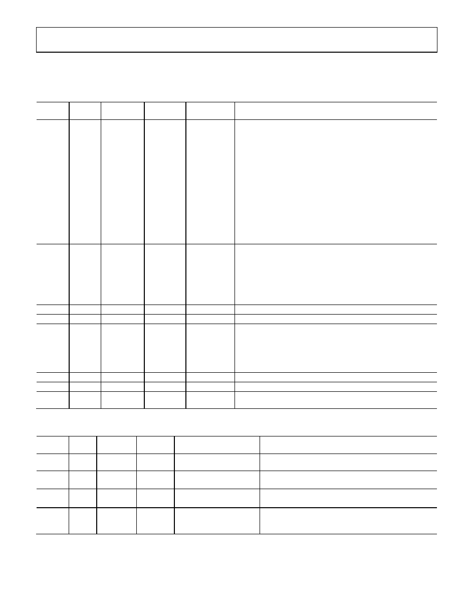
COMPLETE REGISTER LISTING
When an address contains fewer than 28 data bits, all remaining bits must be written as 0s.
Table 29. AFE Registers
Address
Data
Bits
Default
Value
Update
Type
Mnemonic
Description
0x00
[1:0]
3
SCK
STANDBY
Standby modes:
0: Normal operation.
1: Standby1 mode.
2: Standby2 mode.
3: Standby3 mode.
[2]
1
CLPENABLE
0: Disable OB clamp.
1: Enable OB clamp.
[3]
0
CLPSPEED
0: Select normal OB clamp settling.
1: Select fast OB clamp settling.
[4]
0
FASTUPDATE
0: Ignore CDS gain.
1: Very fast clamping when CDS gain is updated.
[5]
0
PBLK_LVL
0: Blank data outputs to 0 during PBLK.
1: Blank data outputs to programmed clamp level during PBLK.
[6]
0
DCBYP
0: Enable input dc restore circuit during PBLK.
1: Disable input dc restore circuit during PBLK.
0x01
[0]
0
SCK
DOUTDISABLE
0: Data outputs are driven.
1: Data outputs are three-stated.
[1]
0
DOUTLATCH
0: Latch data outputs using the rising edge of DOUTPHASEP
(DOUTPHASEP register setting).
1: Output latch is transparent.
[2]
0
GRAY_EN
1: Enable gray encoding of the digital data outputs.
[3]
1
TEST
Set to 0.
0x02
[0]
0
SCK
TEST
Do not access, or set to 0.
0x03
[23:0]
FFFFFF
SCK
TEST
Do not access, or set to 0xFFFFFF.
0x04
[2:0]
0
VD
CDSGAIN
CDS gain setting:
0: 3 dB.
4: 0 dB.
6: +3 dB.
7: +6 dB.
All other values are invalid.
0x05
[9:0]
F
VD
VGAGAIN
VGA gain, 6 dB to 42 dB (0.035 dB per step).
0x06
[9:0]
1EC
VD
CLAMPLEVEL
Optical black clamp level, 0 to 1023 LSB (1 LSB per step).
0x0D
[0]
0
VD
CLIDIVIDE
0: No division of CLI.
1: Divide CLI input frequency by 2.
Table 30. Miscellaneous Registers
Address
Data
Bits
Default
Value
Update
Type
Mnemonic
Description
0x10
[0]
0
SCK
SW_RST
Software reset. Bit self-clears to 0 when a reset occurs.
1: Reset Address 0x00 to Address 0xFF to default values.
0x11
[0]
0
VD
OUTCONTROL
0: Make all outputs dc inactive.
1: Enable outputs at next VD edge.
0x12
[0]
0
SCK
RSTB_EN
1: Configure SYNC pin as RSTB input signal.
[4:1]
0
TEST
Test mode only. Must be set to 0.
0x13
[0]
1
SCK
SYNCENABLE
1: External synchronization enable (configures Pin D3 as an
input).
[1]
0
SYNCPOL
SYNC active polarity.
相关PDF资料 |
PDF描述 |
|---|---|
| AD9995KCPZ | IC CCD SIGNAL PROCESSOR 56-LFCSP |
| ADA4424-6ARUZ | IC FILTR VID6CH SD/ED/HD 38TSSOP |
| ADATE302-02BBCZ | IC DCL ATE 500MHZ DUAL 84CSPBGA |
| ADATE304BBCZ | IC DCL ATE 200MHZ DUAL 84CSPBGA |
| ADATE305BSVZ | IC DCL ATE 250MHZ DUAL 100TQFP |
相关代理商/技术参数 |
参数描述 |
|---|---|
| AD9993BBCZ | 功能描述:IC MIXED-SIGNAL FRONT END 196BGA 制造商:analog devices inc. 系列:- 包装:托盘 零件状态:在售 类型:ADC,DAC 输入类型:LVDS 输出类型:LVDS 接口:SPI 电流 - 电源:- 工作温度:- 安装类型:表面贴装 封装/外壳:196-LFBGA,CSPBGA 供应商器件封装:196-CSPBGA(12x12) 标准包装:1 |
| AD9993BBCZRL | 功能描述:IC MIXED-SIGNAL FRONT END 196BGA 制造商:analog devices inc. 系列:- 包装:带卷(TR) 零件状态:在售 类型:ADC,DAC 输入类型:LVDS 输出类型:LVDS 接口:SPI 电流 - 电源:- 工作温度:- 安装类型:表面贴装 封装/外壳:196-LFBGA,CSPBGA 供应商器件封装:196-CSPBGA(12x12) 标准包装:1,500 |
| AD9993-EBZ | 功能描述:EVAL BOARD MXFE AD9993 制造商:analog devices inc. 系列:* 零件状态:在售 标准包装:1 |
| AD9994 | 制造商:AD 制造商全称:Analog Devices 功能描述:12-Bit CCD Signal Processor with Precision Timing Generator |
| AD9994BCP | 制造商:Analog Devices 功能描述:AFE GEN PURPOSE 12-BIT 64LFCSP - Bulk |
发布紧急采购,3分钟左右您将得到回复。