- 您现在的位置:买卖IC网 > PDF目录10950 > ADAV801ASTZ (Analog Devices Inc)IC CODEC AUDIO R-DVD 3.3V 64LQFP PDF资料下载
参数资料
| 型号: | ADAV801ASTZ |
| 厂商: | Analog Devices Inc |
| 文件页数: | 24/60页 |
| 文件大小: | 0K |
| 描述: | IC CODEC AUDIO R-DVD 3.3V 64LQFP |
| 标准包装: | 1 |
| 类型: | 音频编解码器 |
| 数据接口: | 串行 |
| 分辨率(位): | 24 b |
| ADC / DAC 数量: | 2 / 2 |
| 三角积分调变: | 无 |
| 动态范围,标准 ADC / DAC (db): | 102 / 101 |
| 电压 - 电源,模拟: | 3 V ~ 3.6 V |
| 电压 - 电源,数字: | 3 V ~ 3.6 V |
| 工作温度: | -40°C ~ 85°C |
| 安装类型: | 表面贴装 |
| 封装/外壳: | 64-LQFP |
| 供应商设备封装: | 64-LQFP(10x10) |
| 包装: | 托盘 |
| 配用: | EVAL-ADAV801EBZ-ND - BOARD EVALUATION FOR ADAV801 |
第1页第2页第3页第4页第5页第6页第7页第8页第9页第10页第11页第12页第13页第14页第15页第16页第17页第18页第19页第20页第21页第22页第23页当前第24页第25页第26页第27页第28页第29页第30页第31页第32页第33页第34页第35页第36页第37页第38页第39页第40页第41页第42页第43页第44页第45页第46页第47页第48页第49页第50页第51页第52页第53页第54页第55页第56页第57页第58页第59页第60页
ADAV801
Rev. A | Page 30 of 60
INTERFACE CONTROL
The ADAV801 has a dedicated control port to allow access to
the internal registers of the ADAV801. Each of the internal
registers is eight bits wide. Where bits are described as reserved
(RES), these bits should be programmed as zero.
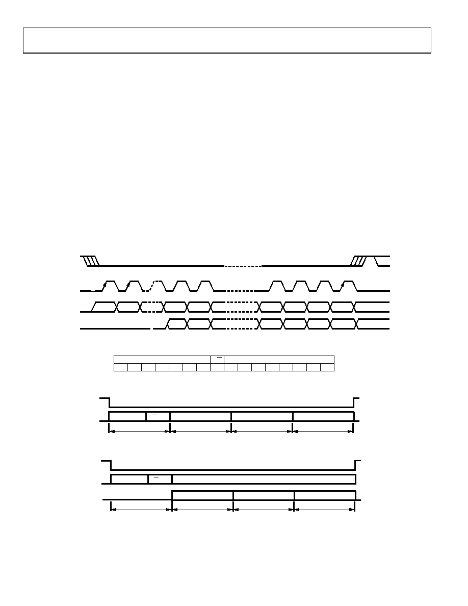
SPI INTERFACE
Control of the ADAV801 is via an SPI-compatible serial port.
The SPI control port is a 4-wire serial control port with one
cycle of data transfer consisting of 16 bits. Figure 53 shows the
format of an SPI write/read of the ADAV801. The transfer of
data is initiated on the falling edge of CLATCH. The data
presented on the first seven CCLKs represents the register
address read/write bit. If this bit is low, the following eight bits
of data are loaded to the register address provided. If this bit is
high, a read operation is indicated. The contents of the register
address are clocked out on the COUT pin on the following eight
CCLKs. For a read operation, the data bits after the read/write
bits are ignored.
BLOCK READS AND WRITES
The ADAV801 provides the user with the ability to write to or
read from a block of registers in one continuous operation. In
SPI mode, the CLATCH line should be held low for longer than
the 16 CCLK periods to use the block read/write mode. For a
write operation, once the LSB has been clocked into the
ADAV801 on the 16th CCLK, the register address as specified
by the first seven bits of the write operation is incremented and
the next eight bits are clocked into the next register address.
The read operation is similar. Once the LSB of a read register
operation has been clocked out, the register address is
incremented and the data from the next register is clocked out
timing diagrams for the block write and read operations.
CLATCH
CCLK
CIN
COUT
D0
D8
D0
D15
D14
D9
D8
D9
0
45
77
-0
33
Figure 53. SPI Serial Port Timing Diagram
14
13
12
11
10
9
876543210
R/W
15
ADDRESS [6:0]
DATA [7:0]
04
57
7-
03
6
Figure 54. SPI Control Word Format
0
45
77-
0
34
REGISTER
REGISTER DATA
REGISTER + 1 DATA
REGISTER + 2 DATA
R/W = 0
8 BITS
CLATCH
CIN
Figure 55. SPI Block Write Operation
0
45
77
-03
5
REGISTER
REGISTER DATA
REGISTER + 1 DATA
REGISTER + 2 DATA
R/W = 1
8 BITS
CLATCH
CIN
DON’T CARE
COUT
Figure 56. SPI Block Read Operation
相关PDF资料 |
PDF描述 |
|---|---|
| MCIMX27LVOP4AR2 | IC LOW END I.MX27 404-MAPBGA |
| AD1938YSTZ | IC CODEC 24BIT 4ADC/8DAC 48LQFP |
| MC56F8335MFGE | IC DIGITAL SIGNAL CTLR 128-LQFP |
| MC9S12XHZ512CAG | IC MCU 16BIT 512 FLASH 144-LQFP |
| MC9S12C96MPBE | IC MCU 96K FLASH 4K RAM 52-LQFP |
相关代理商/技术参数 |
参数描述 |
|---|---|
| ADAV801ASTZ-REEL | 功能描述:IC CODEC AUDIO R-DVD 3.3V 64LQFP RoHS:是 类别:集成电路 (IC) >> 接口 - 编解码器 系列:- 标准包装:2,500 系列:- 类型:立体声音频 数据接口:串行 分辨率(位):18 b ADC / DAC 数量:2 / 2 三角积分调变:是 S/N 比,标准 ADC / DAC (db):81.5 / 88 动态范围,标准 ADC / DAC (db):82 / 87.5 电压 - 电源,模拟:2.6 V ~ 3.3 V 电压 - 电源,数字:1.7 V ~ 3.3 V 工作温度:-40°C ~ 85°C 安装类型:表面贴装 封装/外壳:48-WFQFN 裸露焊盘 供应商设备封装:48-TQFN-EP(7x7) 包装:带卷 (TR) |
| ADAV802AST | 制造商:Analog Devices 功能描述:AUDIO CODEC FOR RECORDABLE DVD - Bulk |
| ADAV802ASTZ | 制造商:Analog Devices 功能描述: |
| ADAV803 | 制造商:AD 制造商全称:Analog Devices 功能描述:Audio Codec for Recordable DVD |
| ADAV803AST | 制造商:Analog Devices 功能描述:AUDIO CODEC FOR RECORDABLE DVD - Bulk |
发布紧急采购,3分钟左右您将得到回复。