- 您现在的位置:买卖IC网 > PDF目录9218 > ADF4350BCPZ-RL7 (Analog Devices Inc)IC SYNTH PLL VCO FN/IN 32LFCSP PDF资料下载
参数资料
| 型号: | ADF4350BCPZ-RL7 |
| 厂商: | Analog Devices Inc |
| 文件页数: | 14/32页 |
| 文件大小: | 0K |
| 描述: | IC SYNTH PLL VCO FN/IN 32LFCSP |
| 产品变化通告: | ADF4350, ADF4905/6 N-counter Change 05/Mar/2012 |
| 设计资源: | Broadband Low EVM Direct Conversion Transmitter (CN0134) Broadband Low EVM Direct Conversion Transmitter Using LO Divide-by-2 Modulator (CN0144) Using low noise linear drop-out regulators to power wideband PLL & VCO IC's (CN0147) |
| 特色产品: | ADF4350: Wideband PLL Synthesizer with integrated VCO |
| 标准包装: | 1 |
| 类型: | 扇出配送,分数-N,整数-N,时钟/频率合成器(RF) |
| PLL: | 是 |
| 输入: | CMOS |
| 输出: | 时钟 |
| 电路数: | 1 |
| 比率 - 输入:输出: | 1:3 |
| 差分 - 输入:输出: | 无/无 |
| 频率 - 最大: | 4.4GHz |
| 除法器/乘法器: | 是/是 |
| 电源电压: | 3 V ~ 3.6 V |
| 工作温度: | -40°C ~ 85°C |
| 安装类型: | 表面贴装 |
| 封装/外壳: | 32-VFQFN 裸露焊盘,CSP |
| 供应商设备封装: | 32-LFCSP-VQ(5x5) |
| 包装: | 标准包装 |
| 产品目录页面: | 551 (CN2011-ZH PDF) |
| 其它名称: | ADF4350BCPZ-RL7DKR |
第1页第2页第3页第4页第5页第6页第7页第8页第9页第10页第11页第12页第13页当前第14页第15页第16页第17页第18页第19页第20页第21页第22页第23页第24页第25页第26页第27页第28页第29页第30页第31页第32页
ADF4350
Rev. A | Page 21 of 32
INITIALIZATION SEQUENCE
The following sequence of registers is the correct sequence for
initial power-up of the ADF4350 after the correct application of
voltages to the supply pins:
Register 5
Register 4
Register 3
Register 2
Register 1
Register 0
RF SYNTHESIZER—A WORKED EXAMPLE
The following is an example how to program the ADF4350
synthesizer:
RFOUT = [INT + (FRAC/MOD)] × [fPFD]/RF divider
(3)
where:
RFOUT is the RF frequency output.
INT is the integer division factor.
FRAC is the fractionality.
MOD is the modulus.
RF divider is the output divider that divides down the VCO
frequency.
fPFD = REFIN × [(1 + D)/(R × (1+T))]
(4)
where:
REFIN is the reference frequency input.
D is the RF REFIN doubler bit.
T is the reference divide-by-2 bit (0 or 1).
R is the RF reference division factor.
For example, in a UMTS system, where 2112.6 MHz RF
frequency output (RFOUT) is required, a 10 MHz reference
frequency input (REFIN) is available, and a 200 kHz channel
resolution (fRESOUT) is required on the RF output. Note that
the ADF4350 operates in the frequency range of 2.2 GHz to
4.4 GHz. Therefore, the RF divider of 2 should be used (VCO
frequency = 4225.2 MHz, RFOUT = VCO frequency/RF divider =
4225.2 MHz/2 = 2112.6 MHz).
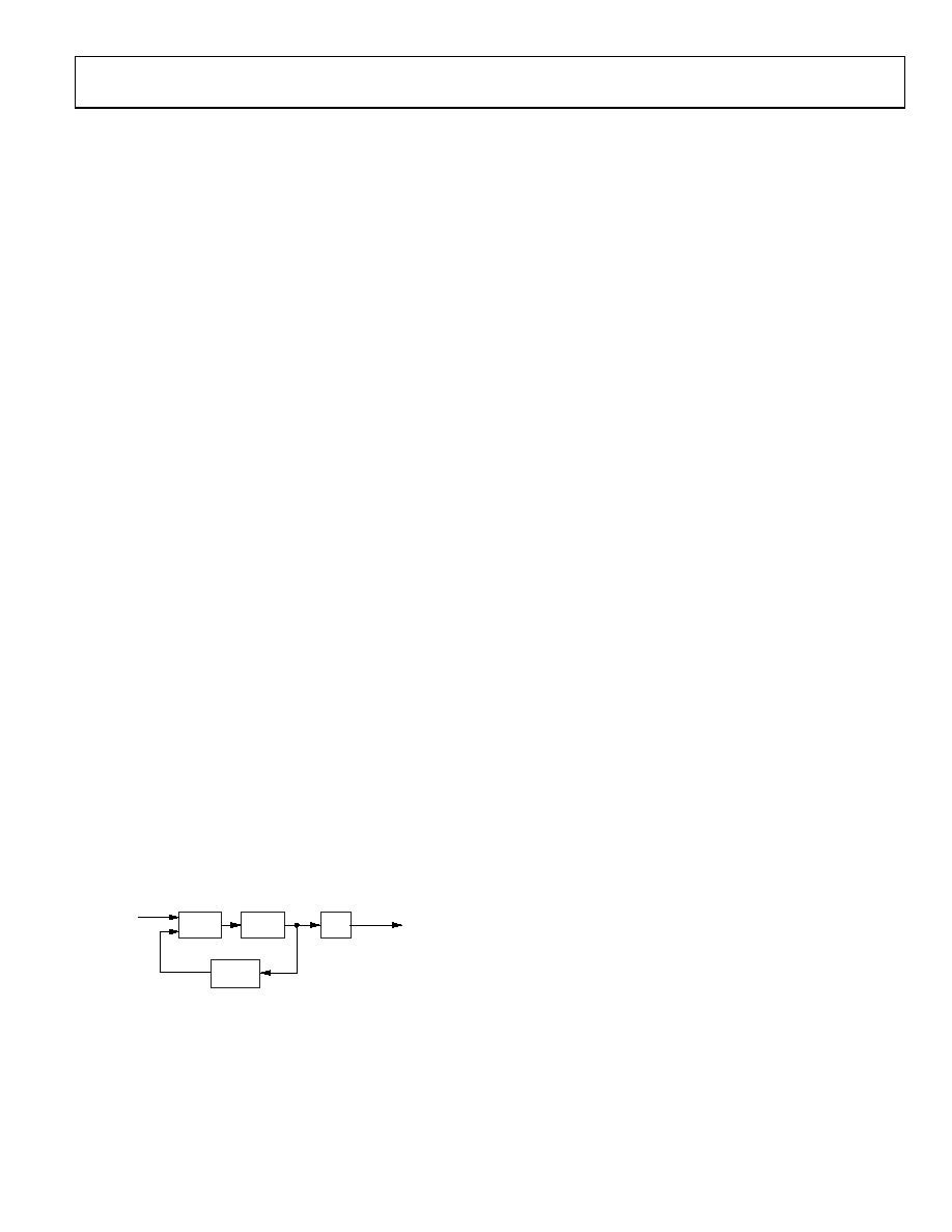
It is also important where the loop is closed. In this example,
the loop is closed (see Figure 30).
fPFD
PFD
VCO
N
DIVIDER
÷2
0
73
25-
0
27
RFOUT
Figure 30. Loop Closed Before Output Divider
Channel resolution (fRESOUT) or 200 kHz is required at the output
of the RF divider. Therefore, channel resolution at the output of
the VCO (fRES) is to be twice the fRESOUT, that is 400 kHz.
MOD = REFIN/fRES
MOD = 10 MHz/400 kHz = 25
From Equation 4,
fPFD = [10 MHz × (1 + 0)/1] = 10 MHz
(5)
2112.6 MHz = 10 MHz × (INT + FRAC/25)/2
(6)
where:
INT = 422
FRAC = 13
MODULUS
The choice of modulus (MOD) depends on the reference signal
(REFIN) available and the channel resolution (fRES) required at
the RF output. For example, a GSM system with 13 MHz REFIN
sets the modulus to 65. This means the RF output resolution (fRES)
is the 200 kHz (13 MHz/65) necessary for GSM. With dither off,
the fractional spur interval depends on the modulus values chosen
(see Table 6).
REFERENCE DOUBLER AND REFERENCE DIVIDER
The reference doubler on-chip allows the input reference signal
to be doubled. This is useful for increasing the PFD comparison
frequency. Making the PFD frequency higher improves the
noise performance of the system. Doubling the PFD frequency
usually improves noise performance by 3 dB. It is important to
note that the PFD cannot operate above 32 MHz due to a limi-
tation in the speed of the Σ-Δ circuit of the N-divider.
The reference divide-by-2 divides the reference signal by 2,
resulting in a 50% duty cycle PFD frequency. This is necessary
for the correct operation of the cycle slip reduction (CSR)
function. See the Cycle Slip Reduction for Faster Lock Times
section for more information.
12-BIT PROGRAMMABLE MODULUS
Unlike most other fractional-N PLLs, the ADF4350 allows the
user to program the modulus over a 12–bit range. This means
the user can set up the part in many different configurations for
the application, when combined with the reference doubler and
the 10-bit R counter.
For example, consider an application that requires 1.75 GHz RF
and 200 kHz channel step resolution. The system has a 13 MHz
reference signal.
One possible setup is feeding the 13 MHz directly to the PFD
and programming the modulus to divide by 65. This results in
the required 200 kHz resolution.
Another possible setup is using the reference doubler to create
26 MHz from the 13 MHz input signal. This 26 MHz is then fed
into the PFD programming the modulus to divide by 130. This
also results in 200 kHz resolution and offers superior phase
noise performance over the previous setup.
相关PDF资料 |
PDF描述 |
|---|---|
| SY100E457JZ | IC MUX TRIPLE DIFF 2:1 28-PLCC |
| SY100E164JZ | IC MULTIPLEXER 16:1 28-PLCC |
| X9317US8IZ-2.7 | IC XDCP 100TAP 50K 3-WIRE 8-SOIC |
| SY58030UMG TR | IC MUX DIFF LVPECL 4:1 32-MLF |
| VE-JVY-MZ-S | CONVERTER MOD DC/DC 3.3V 16.5W |
相关代理商/技术参数 |
参数描述 |
|---|---|
| ADF4350BCPZ-U6 | 制造商:Analog Devices 功能描述: |
| ADF4350EB1Z | 制造商:Analog Devices 功能描述:AD EVAL BOARD - Bulk |
| ADF4351 | 制造商:AD 制造商全称:Analog Devices 功能描述:Wideband Synthesizer |
| ADF4351BCPZ | 功能描述:IC SYNTH PLL VCO 32LFCSP RoHS:是 类别:集成电路 (IC) >> 时钟/计时 - 时钟发生器,PLL,频率合成器 系列:- 标准包装:2,000 系列:- 类型:PLL 时钟发生器 PLL:带旁路 输入:LVCMOS,LVPECL 输出:LVCMOS 电路数:1 比率 - 输入:输出:2:11 差分 - 输入:输出:是/无 频率 - 最大:240MHz 除法器/乘法器:是/无 电源电压:3.135 V ~ 3.465 V 工作温度:0°C ~ 70°C 安装类型:表面贴装 封装/外壳:32-LQFP 供应商设备封装:32-TQFP(7x7) 包装:带卷 (TR) |
| ADF4351BCPZ-RL7 | 功能描述:IC SYNTH PLL VCO 32LFCSP RoHS:是 类别:集成电路 (IC) >> 时钟/计时 - 时钟发生器,PLL,频率合成器 系列:- 标准包装:2,000 系列:- 类型:PLL 时钟发生器 PLL:带旁路 输入:LVCMOS,LVPECL 输出:LVCMOS 电路数:1 比率 - 输入:输出:2:11 差分 - 输入:输出:是/无 频率 - 最大:240MHz 除法器/乘法器:是/无 电源电压:3.135 V ~ 3.465 V 工作温度:0°C ~ 70°C 安装类型:表面贴装 封装/外壳:32-LQFP 供应商设备封装:32-TQFP(7x7) 包装:带卷 (TR) |
发布紧急采购,3分钟左右您将得到回复。