- 您现在的位置:买卖IC网 > PDF目录9218 > ADF4350BCPZ-RL7 (Analog Devices Inc)IC SYNTH PLL VCO FN/IN 32LFCSP PDF资料下载
参数资料
| 型号: | ADF4350BCPZ-RL7 |
| 厂商: | Analog Devices Inc |
| 文件页数: | 4/32页 |
| 文件大小: | 0K |
| 描述: | IC SYNTH PLL VCO FN/IN 32LFCSP |
| 产品变化通告: | ADF4350, ADF4905/6 N-counter Change 05/Mar/2012 |
| 设计资源: | Broadband Low EVM Direct Conversion Transmitter (CN0134) Broadband Low EVM Direct Conversion Transmitter Using LO Divide-by-2 Modulator (CN0144) Using low noise linear drop-out regulators to power wideband PLL & VCO IC's (CN0147) |
| 特色产品: | ADF4350: Wideband PLL Synthesizer with integrated VCO |
| 标准包装: | 1 |
| 类型: | 扇出配送,分数-N,整数-N,时钟/频率合成器(RF) |
| PLL: | 是 |
| 输入: | CMOS |
| 输出: | 时钟 |
| 电路数: | 1 |
| 比率 - 输入:输出: | 1:3 |
| 差分 - 输入:输出: | 无/无 |
| 频率 - 最大: | 4.4GHz |
| 除法器/乘法器: | 是/是 |
| 电源电压: | 3 V ~ 3.6 V |
| 工作温度: | -40°C ~ 85°C |
| 安装类型: | 表面贴装 |
| 封装/外壳: | 32-VFQFN 裸露焊盘,CSP |
| 供应商设备封装: | 32-LFCSP-VQ(5x5) |
| 包装: | 标准包装 |
| 产品目录页面: | 551 (CN2011-ZH PDF) |
| 其它名称: | ADF4350BCPZ-RL7DKR |
第1页第2页第3页当前第4页第5页第6页第7页第8页第9页第10页第11页第12页第13页第14页第15页第16页第17页第18页第19页第20页第21页第22页第23页第24页第25页第26页第27页第28页第29页第30页第31页第32页
ADF4350
Rev. A | Page 12 of 32
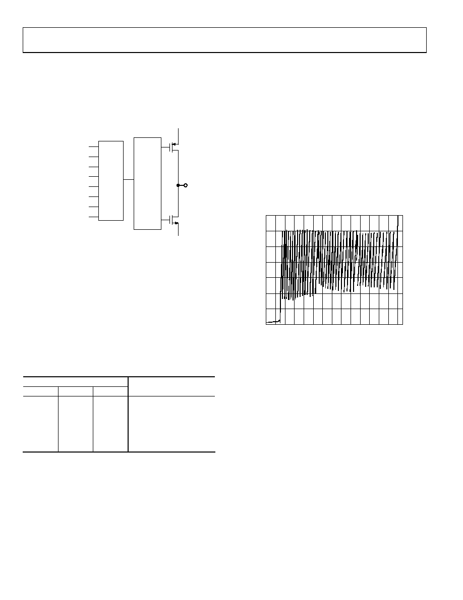
MUXOUT AND LOCK DETECT
The output multiplexer on the ADF4350 allows the user
to access various internal points on the chip. The state of
MUXOUT is controlled by M3, M2, and M1 (for details,
block diagram form.
DGND
DVDD
CONTROL
MUX
MUXOUT
ANALOG LOCK DETECT
DIGITAL LOCK DETECT
R COUNTER OUTPUT
N COUNTER OUTPUT
DGND
RESERVED
THREE-STATE OUTPUT
DVDD
Figure 19. MUXOUT Schematic
INPUT SHIFT REGISTERS
The ADF4350 digital section includes a 10–bit RF R counter,
a 16–bit RF N counter, a 12-bit FRAC counter, and a 12–bit
modulus counter. Data is clocked into the 32–bit shift register
on each rising edge of CLK. The data is clocked in MSB first.
Data is transferred from the shift register to one of six latches
on the rising edge of LE. The destination latch is determined by
the state of the three control bits (C3, C2, and C1) in the shift
register. These are the 3 LSBs, DB2, DB1, and DB0, as shown
in Figure 2. The truth table for these bits is shown in Table 5.
Figure 23 shows a summary of how the latches are programmed.
Table 5. C3, C2, and C1 Truth Table
Control Bits
C3
C2
C1
Register
0
Register 0 (R0)
0
1
Register 1 (R1)
0
1
0
Register 2 (R2)
0
1
Register 3 (R3)
1
0
Register 4 (R4)
1
0
1
Register 5 (R5)
PROGRAM MODES
modes are to be set up in the ADF4350.
A number of settings in the ADF4350 are double buffered.
These include the modulus value, phase value, R counter value,
reference doubler, reference divide-by-2, and current setting.
This means that two events have to occur before the part uses
a new value of any of the double buffered settings. First, the
new value is latched into the device by writing to the appropriate
register. Second, a new write must be performed on Register R0.
For example, any time the modulus value is updated, Register 0
(R0) must be written to, to ensure the modulus value is loaded
correctly. Divider select in Register 4 (R4) is also double buf-
fered, but only if DB13 of Register 2 (R2) is high.
VCO
The VCO core in the ADF4350 consists of three separate VCOs
each of which uses 16 overlapping bands, as shown in Figure 20,
to allow a wide frequency range to be covered without a large
VCO sensitivity (KV) and resultant poor phase noise and spu-
rious performance.
The correct VCO and band are chosen automatically by the
VCO and band select logic at power-up or whenever Register 0
(R0) is updated.
VCO and band selection take 10 PFD cycles × band select clock
divider value. The VCO VTUNE is disconnected from the output
of the loop filter and is connected to an internal reference voltage.
2.8
2.4
2.0
1.6
0.8
1.2
0.4
0
1800
2000
2200
2400
2600
2800
3000
3200
3400
3600
3800
4000
4200
4400
4600
07
32
5-
0
09
FREQUENCY (MHz)
V
TU
NE
(V
)
Figure 20. VTUNE vs. Frequency
The R counter output is used as the clock for the band select
logic. A programmable divider is provided at the R counter
output to allow division by 1 to 255 and is controlled by
Bits [BS8:BS1] in Register 4 (R4). When the required PFD
frequency is higher than 125 kHz, the divide ratio should be
set to allow enough time for correct band selection.
After band select, normal PLL action resumes. The nominal
value of KV is 33 MHz/V when the N-divider is driven from the
VCO output or this value divided by D. D is the output divider
value if the N-divider is driven from the RF divider output
(chosen by programming Bits [D12:D10] in Register 4 (R4).
The ADF4350 contains linearization circuitry to minimize
any variation of the product of ICP and KV to keep the loop
bandwidth constant.
相关PDF资料 |
PDF描述 |
|---|---|
| SY100E457JZ | IC MUX TRIPLE DIFF 2:1 28-PLCC |
| SY100E164JZ | IC MULTIPLEXER 16:1 28-PLCC |
| X9317US8IZ-2.7 | IC XDCP 100TAP 50K 3-WIRE 8-SOIC |
| SY58030UMG TR | IC MUX DIFF LVPECL 4:1 32-MLF |
| VE-JVY-MZ-S | CONVERTER MOD DC/DC 3.3V 16.5W |
相关代理商/技术参数 |
参数描述 |
|---|---|
| ADF4350BCPZ-U6 | 制造商:Analog Devices 功能描述: |
| ADF4350EB1Z | 制造商:Analog Devices 功能描述:AD EVAL BOARD - Bulk |
| ADF4351 | 制造商:AD 制造商全称:Analog Devices 功能描述:Wideband Synthesizer |
| ADF4351BCPZ | 功能描述:IC SYNTH PLL VCO 32LFCSP RoHS:是 类别:集成电路 (IC) >> 时钟/计时 - 时钟发生器,PLL,频率合成器 系列:- 标准包装:2,000 系列:- 类型:PLL 时钟发生器 PLL:带旁路 输入:LVCMOS,LVPECL 输出:LVCMOS 电路数:1 比率 - 输入:输出:2:11 差分 - 输入:输出:是/无 频率 - 最大:240MHz 除法器/乘法器:是/无 电源电压:3.135 V ~ 3.465 V 工作温度:0°C ~ 70°C 安装类型:表面贴装 封装/外壳:32-LQFP 供应商设备封装:32-TQFP(7x7) 包装:带卷 (TR) |
| ADF4351BCPZ-RL7 | 功能描述:IC SYNTH PLL VCO 32LFCSP RoHS:是 类别:集成电路 (IC) >> 时钟/计时 - 时钟发生器,PLL,频率合成器 系列:- 标准包装:2,000 系列:- 类型:PLL 时钟发生器 PLL:带旁路 输入:LVCMOS,LVPECL 输出:LVCMOS 电路数:1 比率 - 输入:输出:2:11 差分 - 输入:输出:是/无 频率 - 最大:240MHz 除法器/乘法器:是/无 电源电压:3.135 V ~ 3.465 V 工作温度:0°C ~ 70°C 安装类型:表面贴装 封装/外壳:32-LQFP 供应商设备封装:32-TQFP(7x7) 包装:带卷 (TR) |
发布紧急采购,3分钟左右您将得到回复。