- 您现在的位置:买卖IC网 > PDF目录9218 > ADF4350BCPZ-RL7 (Analog Devices Inc)IC SYNTH PLL VCO FN/IN 32LFCSP PDF资料下载
参数资料
| 型号: | ADF4350BCPZ-RL7 |
| 厂商: | Analog Devices Inc |
| 文件页数: | 16/32页 |
| 文件大小: | 0K |
| 描述: | IC SYNTH PLL VCO FN/IN 32LFCSP |
| 产品变化通告: | ADF4350, ADF4905/6 N-counter Change 05/Mar/2012 |
| 设计资源: | Broadband Low EVM Direct Conversion Transmitter (CN0134) Broadband Low EVM Direct Conversion Transmitter Using LO Divide-by-2 Modulator (CN0144) Using low noise linear drop-out regulators to power wideband PLL & VCO IC's (CN0147) |
| 特色产品: | ADF4350: Wideband PLL Synthesizer with integrated VCO |
| 标准包装: | 1 |
| 类型: | 扇出配送,分数-N,整数-N,时钟/频率合成器(RF) |
| PLL: | 是 |
| 输入: | CMOS |
| 输出: | 时钟 |
| 电路数: | 1 |
| 比率 - 输入:输出: | 1:3 |
| 差分 - 输入:输出: | 无/无 |
| 频率 - 最大: | 4.4GHz |
| 除法器/乘法器: | 是/是 |
| 电源电压: | 3 V ~ 3.6 V |
| 工作温度: | -40°C ~ 85°C |
| 安装类型: | 表面贴装 |
| 封装/外壳: | 32-VFQFN 裸露焊盘,CSP |
| 供应商设备封装: | 32-LFCSP-VQ(5x5) |
| 包装: | 标准包装 |
| 产品目录页面: | 551 (CN2011-ZH PDF) |
| 其它名称: | ADF4350BCPZ-RL7DKR |
第1页第2页第3页第4页第5页第6页第7页第8页第9页第10页第11页第12页第13页第14页第15页当前第16页第17页第18页第19页第20页第21页第22页第23页第24页第25页第26页第27页第28页第29页第30页第31页第32页
ADF4350
Rev. A | Page 23 of 32
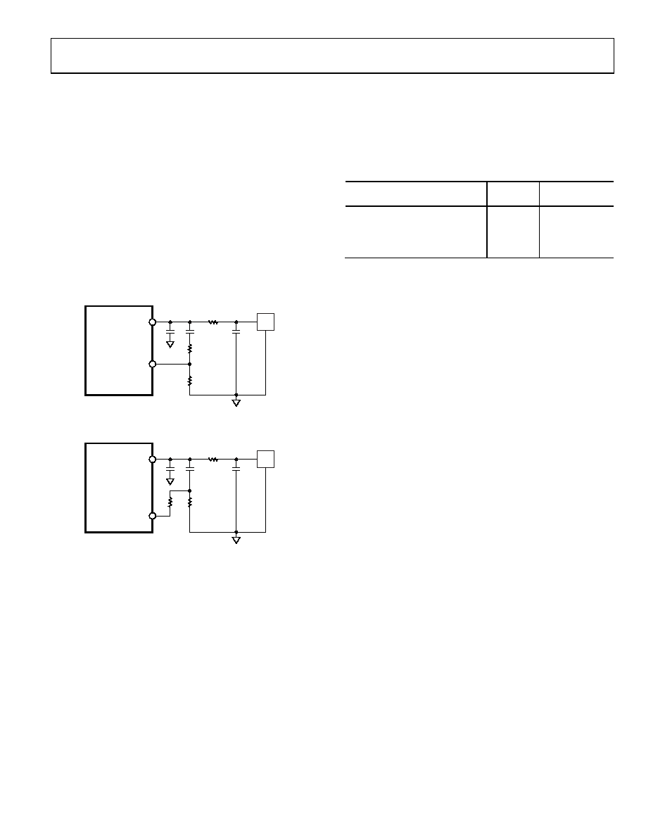
FAST LOCK—LOOP FILTER TOPOLOGY
To use fast-lock mode, the damping resistor in the loop filter
is reduced to of its value while in wide bandwidth mode. To
achieve the wider loop filter bandwidth, the charge pump
current increases by a factor of 16 and to maintain loop sta-
bility the damping resistor must be reduced a factor of .
To enable fast lock, the SW pin is shorted to the GND pin by
settings Bits [DB16:DB15] in Register 3 to 0, 1. The following
two topologies are available:
The damping resistor (R1) is divided into two values (R1
and R1A) that have a ratio of 1:3 (see Figure 31).
An extra resistor (R1A) is connected directly from SW, as
shown in Figure 32. The extra resistor is calculated such
that the parallel combination of an extra resistor and the
damping resistor (R1) is reduced to of the original value
of R1 (see Figure 32).
ADF4350
CP
SW
C1
C2
R2
R1
R1A
C3
VCO
0
732
5-
0
18
Figure 31. Fast-Lock Loop Filter Topology—Topology 1
ADF4350
CP
SW
C1
C2
R2
R1
R1A
C3
VCO
0
732
5-
0
19
Figure 32. Fast-Lock Loop Filter Topology—Topology 2
SPUR MECHANISMS
This section describes the three different spur mechanisms that
arise with a fractional-N synthesizer and how to minimize them
in the ADF4350.
Fractional Spurs
The fractional interpolator in the ADF4350 is a third-order
Σ-Δ modulator (SDM) with a modulus (MOD) that is program-
mable to any integer value from 2 to 4095. In low spur mode
(dither enabled) the minimum allowable value of MOD is 50.
The SDM is clocked at the PFD reference rate (fPFD) that allows
PLL output frequencies to be synthesized at a channel step
resolution of fPFD/MOD.
In low noise mode (dither disabled) the quantization noise from
the Σ-Δ modulator appears as fractional spurs. The interval
between spurs is fPFD/L, where L is the repeat length of the code
sequence in the digital Σ-Δ modulator. For the third-order
modulator used in the ADF4350, the repeat length depends on
the value of MOD, as listed in Table 6.
Table 6. Fractional Spurs with Dither Disabled
Condition (Dither Disabled)
Repeat
Length
Spur Interval
If MOD is divisible by 2, but not 3
2 × MOD
Channel step/2
If MOD is divisible by 3, but not 2
3 × MOD
Channel step/3
If MOD is divisible by 6
6 × MOD
Channel step/6
Otherwise
MOD
Channel step
In low spur mode (dither enabled), the repeat length is extend-
ed to 221 cycles, regardless of the value of MOD, which makes
the quantization error spectrum look like broadband noise.
This may degrade the in-band phase noise at the PLL output
by as much as 10 dB. For lowest noise, dither disabled is a better
choice, particularly when the final loop bandwidth is low
enough to attenuate even the lowest frequency fractional spur.
Integer Boundary Spurs
Another mechanism for fractional spur creation is the inter-
actions between the RF VCO frequency and the reference
frequency. When these frequencies are not integer related (the
point of a fractional-N synthesizer) spur sidebands appear on
the VCO output spectrum at an offset frequency that corres-
ponds to the beat note or difference frequency between an
integer multiple of the reference and the VCO frequency. These
spurs are attenuated by the loop filter and are more noticeable
on channels close to integer multiples of the reference where the
difference frequency can be inside the loop bandwidth, there-
fore, the name integer boundary spurs.
Reference Spurs
Reference spurs are generally not a problem in fractional-N
synthesizers because the reference offset is far outside the loop
bandwidth. However, any reference feed-through mechanism
that bypasses the loop may cause a problem. Feed through of
low levels of on-chip reference switching noise, through the
RFIN pin back to the VCO, can result in reference spur levels as
high as –90 dBc. PCB layout needs to ensure adequate isolation
between VCO traces and the input reference to avoid a possible
feed through path on the board.
相关PDF资料 |
PDF描述 |
|---|---|
| SY100E457JZ | IC MUX TRIPLE DIFF 2:1 28-PLCC |
| SY100E164JZ | IC MULTIPLEXER 16:1 28-PLCC |
| X9317US8IZ-2.7 | IC XDCP 100TAP 50K 3-WIRE 8-SOIC |
| SY58030UMG TR | IC MUX DIFF LVPECL 4:1 32-MLF |
| VE-JVY-MZ-S | CONVERTER MOD DC/DC 3.3V 16.5W |
相关代理商/技术参数 |
参数描述 |
|---|---|
| ADF4350BCPZ-U6 | 制造商:Analog Devices 功能描述: |
| ADF4350EB1Z | 制造商:Analog Devices 功能描述:AD EVAL BOARD - Bulk |
| ADF4351 | 制造商:AD 制造商全称:Analog Devices 功能描述:Wideband Synthesizer |
| ADF4351BCPZ | 功能描述:IC SYNTH PLL VCO 32LFCSP RoHS:是 类别:集成电路 (IC) >> 时钟/计时 - 时钟发生器,PLL,频率合成器 系列:- 标准包装:2,000 系列:- 类型:PLL 时钟发生器 PLL:带旁路 输入:LVCMOS,LVPECL 输出:LVCMOS 电路数:1 比率 - 输入:输出:2:11 差分 - 输入:输出:是/无 频率 - 最大:240MHz 除法器/乘法器:是/无 电源电压:3.135 V ~ 3.465 V 工作温度:0°C ~ 70°C 安装类型:表面贴装 封装/外壳:32-LQFP 供应商设备封装:32-TQFP(7x7) 包装:带卷 (TR) |
| ADF4351BCPZ-RL7 | 功能描述:IC SYNTH PLL VCO 32LFCSP RoHS:是 类别:集成电路 (IC) >> 时钟/计时 - 时钟发生器,PLL,频率合成器 系列:- 标准包装:2,000 系列:- 类型:PLL 时钟发生器 PLL:带旁路 输入:LVCMOS,LVPECL 输出:LVCMOS 电路数:1 比率 - 输入:输出:2:11 差分 - 输入:输出:是/无 频率 - 最大:240MHz 除法器/乘法器:是/无 电源电压:3.135 V ~ 3.465 V 工作温度:0°C ~ 70°C 安装类型:表面贴装 封装/外壳:32-LQFP 供应商设备封装:32-TQFP(7x7) 包装:带卷 (TR) |
发布紧急采购,3分钟左右您将得到回复。