- 您现在的位置:买卖IC网 > PDF目录9218 > ADF4350BCPZ-RL7 (Analog Devices Inc)IC SYNTH PLL VCO FN/IN 32LFCSP PDF资料下载
参数资料
| 型号: | ADF4350BCPZ-RL7 |
| 厂商: | Analog Devices Inc |
| 文件页数: | 5/32页 |
| 文件大小: | 0K |
| 描述: | IC SYNTH PLL VCO FN/IN 32LFCSP |
| 产品变化通告: | ADF4350, ADF4905/6 N-counter Change 05/Mar/2012 |
| 设计资源: | Broadband Low EVM Direct Conversion Transmitter (CN0134) Broadband Low EVM Direct Conversion Transmitter Using LO Divide-by-2 Modulator (CN0144) Using low noise linear drop-out regulators to power wideband PLL & VCO IC's (CN0147) |
| 特色产品: | ADF4350: Wideband PLL Synthesizer with integrated VCO |
| 标准包装: | 1 |
| 类型: | 扇出配送,分数-N,整数-N,时钟/频率合成器(RF) |
| PLL: | 是 |
| 输入: | CMOS |
| 输出: | 时钟 |
| 电路数: | 1 |
| 比率 - 输入:输出: | 1:3 |
| 差分 - 输入:输出: | 无/无 |
| 频率 - 最大: | 4.4GHz |
| 除法器/乘法器: | 是/是 |
| 电源电压: | 3 V ~ 3.6 V |
| 工作温度: | -40°C ~ 85°C |
| 安装类型: | 表面贴装 |
| 封装/外壳: | 32-VFQFN 裸露焊盘,CSP |
| 供应商设备封装: | 32-LFCSP-VQ(5x5) |
| 包装: | 标准包装 |
| 产品目录页面: | 551 (CN2011-ZH PDF) |
| 其它名称: | ADF4350BCPZ-RL7DKR |
第1页第2页第3页第4页当前第5页第6页第7页第8页第9页第10页第11页第12页第13页第14页第15页第16页第17页第18页第19页第20页第21页第22页第23页第24页第25页第26页第27页第28页第29页第30页第31页第32页
ADF4350
Rev. A | Page 13 of 32
OUTPUT STAGE
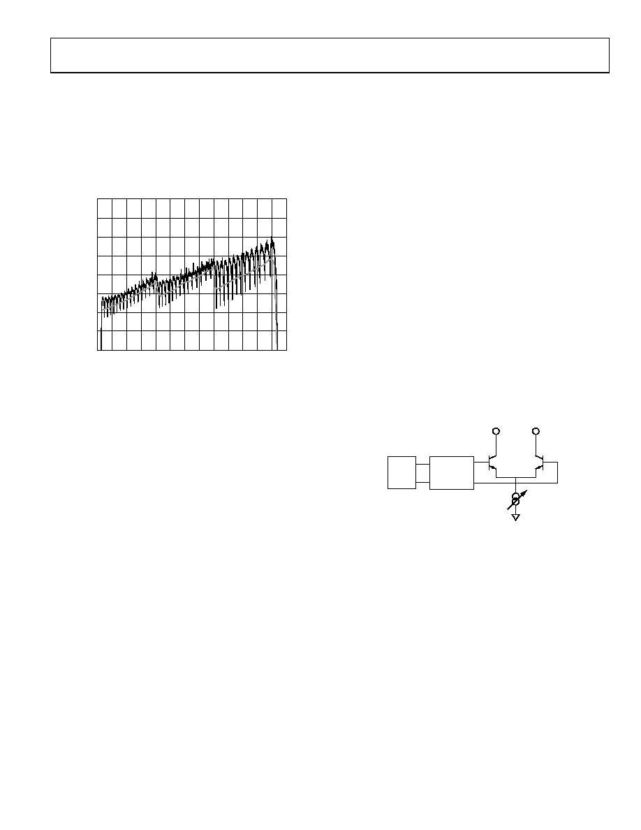
The VCO shows variation of KV as the VTUNE varies within the
band and from band-to-band. It has been shown for wideband
applications covering a wide frequency range (and changing
output dividers) that a value of 33 MHz/V provides the most
shows how KV varies with fundamental VCO frequency along
with an average value for the frequency band. Users may prefer
this figure when using narrowband designs.
The RFOUTA+ and RFOUTA pins of the ADF4350 are connected
to the collectors of an NPN differential pair driven by buffered
outputs of the VCO, as shown in Figure 22. To allow the user to
optimize the power dissipation vs. the output power requirements,
the tail current of the differential pair is programmable by
Bits [D2:D1] in Register 4 (R4). Four current levels may be set.
These levels give output power levels of 4 dBm, 1 dBm, +2
dBm, and +5 dBm, respectively, using a 50 Ω resistor to AVDD
and ac coupling into a 50 Ω load. Alternatively, both outputs
can be combined in a 1 + 1:1 transformer or a 180° microstrip
coupler (see the Output Matching section). If the outputs are
used individually, the optimum output stage consists of a shunt
inductor to VVCO. The unused complementary output must
be terminated with a similar circuit to the used output.
80
70
60
50
40
30
20
10
0
2.0 2.2 2.4 2.6 2.8 3.0 3.2 3.4 3.6 3.8 4.0 4.2 4.4 4.6
07
325
-13
3
VC
O
SEN
SI
T
IVI
T
Y
(M
H
z/
V
)
FREQUENCY (GHz)
An auxiliary output stage exists on Pins RFOUTB+ and RFOUTB
providing a second set of differential outputs which can be
used to drive another circuit, or which can be powered down
if unused. The auxiliary output must be used in conjunction
with the main RF output. It cannot be used with the main
output powered down.
Another feature of the ADF4350 is that the supply current to
the RF output stage can be shut down until the part achieves
lock as measured by the digital lock detect circuitry. This is
enabled by the mute till lock detect (MTLD) bit in Register 4 (R4).
Figure 21. KV vs. Frequency
In fixed frequency applications, the ADF4350 VTUNE may
vary with ambient temperature switching from hot to cold.
In extreme cases, the drift causes VTUNE to drop to a very low
level (<0.25 V) and can cause loss of lock. This becomes an
issue only at fundamental VCO frequencies less than 2.95 GHz
and at ambient temperatures below 0°C.
VCO
RFOUTA+
RFOUTA–
BUFFER/
DIVIDE-BY-
1/2/4/8/16
07
32
5-
0
1
0
In cases such as these, if the ambient temperature decreases
below 0°C, the frequency needs to be reprogrammed (R0 updated)
to avoid VTUNE dropping to a level close to 0 V. Reprogramming
the part chooses a more suitable VCO band, and thus avoids
the low VTUNE issue. Any further temperature drops of more
than 20°C (below 0°C) also require further reprogramming.
Any increases in the ambient temperature do not require repro-
gramming.
Figure 22. Output Stage
相关PDF资料 |
PDF描述 |
|---|---|
| SY100E457JZ | IC MUX TRIPLE DIFF 2:1 28-PLCC |
| SY100E164JZ | IC MULTIPLEXER 16:1 28-PLCC |
| X9317US8IZ-2.7 | IC XDCP 100TAP 50K 3-WIRE 8-SOIC |
| SY58030UMG TR | IC MUX DIFF LVPECL 4:1 32-MLF |
| VE-JVY-MZ-S | CONVERTER MOD DC/DC 3.3V 16.5W |
相关代理商/技术参数 |
参数描述 |
|---|---|
| ADF4350BCPZ-U6 | 制造商:Analog Devices 功能描述: |
| ADF4350EB1Z | 制造商:Analog Devices 功能描述:AD EVAL BOARD - Bulk |
| ADF4351 | 制造商:AD 制造商全称:Analog Devices 功能描述:Wideband Synthesizer |
| ADF4351BCPZ | 功能描述:IC SYNTH PLL VCO 32LFCSP RoHS:是 类别:集成电路 (IC) >> 时钟/计时 - 时钟发生器,PLL,频率合成器 系列:- 标准包装:2,000 系列:- 类型:PLL 时钟发生器 PLL:带旁路 输入:LVCMOS,LVPECL 输出:LVCMOS 电路数:1 比率 - 输入:输出:2:11 差分 - 输入:输出:是/无 频率 - 最大:240MHz 除法器/乘法器:是/无 电源电压:3.135 V ~ 3.465 V 工作温度:0°C ~ 70°C 安装类型:表面贴装 封装/外壳:32-LQFP 供应商设备封装:32-TQFP(7x7) 包装:带卷 (TR) |
| ADF4351BCPZ-RL7 | 功能描述:IC SYNTH PLL VCO 32LFCSP RoHS:是 类别:集成电路 (IC) >> 时钟/计时 - 时钟发生器,PLL,频率合成器 系列:- 标准包装:2,000 系列:- 类型:PLL 时钟发生器 PLL:带旁路 输入:LVCMOS,LVPECL 输出:LVCMOS 电路数:1 比率 - 输入:输出:2:11 差分 - 输入:输出:是/无 频率 - 最大:240MHz 除法器/乘法器:是/无 电源电压:3.135 V ~ 3.465 V 工作温度:0°C ~ 70°C 安装类型:表面贴装 封装/外壳:32-LQFP 供应商设备封装:32-TQFP(7x7) 包装:带卷 (TR) |
发布紧急采购,3分钟左右您将得到回复。