- 您现在的位置:买卖IC网 > PDF目录16743 > ADP1043AACPZ-R7 (Analog Devices Inc)IC THERMO COOLER CTLR 32LFCSP PDF资料下载
参数资料
| 型号: | ADP1043AACPZ-R7 |
| 厂商: | Analog Devices Inc |
| 文件页数: | 9/72页 |
| 文件大小: | 0K |
| 描述: | IC THERMO COOLER CTLR 32LFCSP |
| 标准包装: | 1,500 |
| 应用: | 电源 |
| 输入电压: | 0 V ~ 1.55 V |
| 电源电压: | 3.1 V ~ 3.6 V |
| 电流 - 电源: | 20mA |
| 工作温度: | -40°C ~ 85°C |
| 安装类型: | 表面贴装 |
| 封装/外壳: | 32-VFQFN 裸露焊盘,CSP |
| 供应商设备封装: | 32-LFCSP-VQ(5x5) |
| 包装: | 带卷 (TR) |
第1页第2页第3页第4页第5页第6页第7页第8页当前第9页第10页第11页第12页第13页第14页第15页第16页第17页第18页第19页第20页第21页第22页第23页第24页第25页第26页第27页第28页第29页第30页第31页第32页第33页第34页第35页第36页第37页第38页第39页第40页第41页第42页第43页第44页第45页第46页第47页第48页第49页第50页第51页第52页第53页第54页第55页第56页第57页第58页第59页第60页第61页第62页第63页第64页第65页第66页第67页第68页第69页第70页第71页第72页
�� ��
��
��ADP1043A�
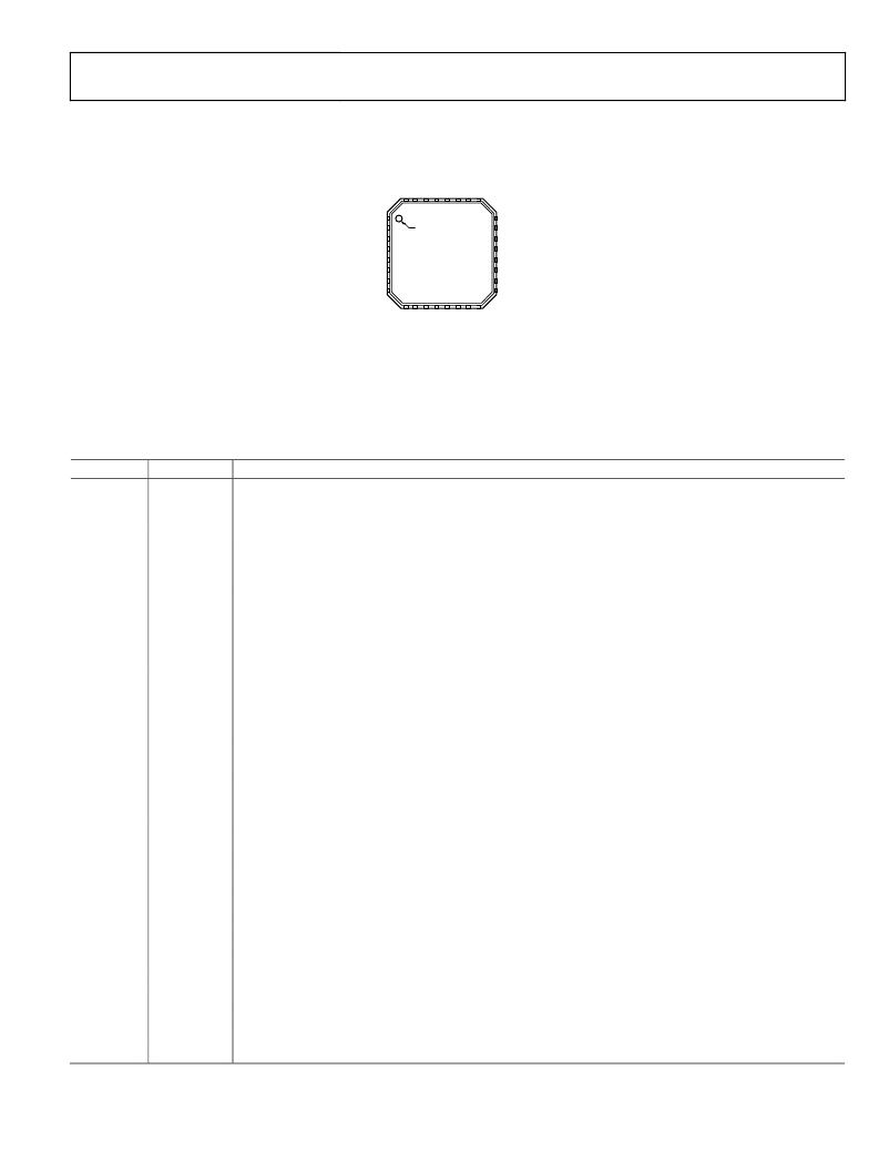
�PIN� CONFIGURATION� AND� FUNCTION� DESCRIPTIONS�
�VS2�
�1�
�24�
�SHAREi�
�AGND�
�VS1�
�CS2–�
�CS2+�
�ACSNS�
�CS1�
�PGND�
�2�
�3�
�4�
�5�
�6�
�7�
�8�
�PIN� 1�
�INDICATOR�
�TOP� VIEW�
�(Not� to� Scale)�
�23�
�22�
�21�
�20�
�19�
�18�
�17�
�SHAREo�
�PGOOD1�
�PGOOD2�
�FLAGIN�
�PSON�
�SDA�
�SCL�
�NOTES�
�1.� THE� ADP1043A� HAS� AN� EXPOSED� THERMAL� PAD� ON� THE� UNDERSIDE�
�OF� THE� PACKAGE.� FOR� INCREASED� RELIABILITY� OF� THE� SOLDER�
�JOINTS� AND� MAXIMUM� THERMAL� CAPABILITY,� IT� IS� RECOMMENDED�
�THAT� THE� PAD� BE� SOLDERED� TO� THE� PCB� GROUND� PLANE.�
�Figure� 3.� Pin� Configuration�
�Table� 4.� Pin� Function� Descriptions�
�Pin� No.�
�1�
�2�
�3�
�4�
�5�
�6�
�7�
�8�
�9�
�10�
�11�
�12�
�13�
�14�
�15�
�16�
�17�
�18�
�Mnemonic�
�VS2�
�AGND�
�VS1�
�CS2?�
�CS2+�
�ACSNS�
�CS1�
�PGND�
�SR1�
�SR2�
�OUTA�
�OUTB�
�OUTC�
�OUTD�
�OUTAUX�
�GATE�
�SCL�
�SDA�
�Description�
�Power� Supply� Output� Sense� Input.� This� signal� is� referred� to� PGND.� Input� to� a� low� frequency� Σ-Δ� ADC.� Nominal�
�voltage� at� this� pin� should� be� 1� V.� The� resistor� divider� on� this� input� must� have� a� tolerance� specification� of� 0.5%�
�or� better� to� allow� for� trimming.�
�Analog� Ground.� This� pin� is� the� ground� for� the� analog� circuitry� of� the� ADP1043A.� Star� connect� to� DGND.�
�Local� Voltage� Sense� Input.� This� signal� is� referred� to� PGND.� Input� to� a� high� frequency� Σ-Δ� ADC.� Nominal� voltage�
�at� this� pin� should� be� 1� V.� The� resistor� divider� on� this� input� must� have� a� tolerance� specification� of� 0.5%� or�
�better� to� allow� for� trimming.�
�Inverting� Differential� Current� Sense� Input.� Nominal� voltage� at� this� pin� should� be� 1� V� for� best� operation.� When�
�using� high-side� current� sensing� in� a� 12� V� application,� place� a� 110� k� resistor� between� the� sense� resistor� and�
�this� pin.� When� using� low-side� current� sensing,� place� a� 10� k� resistor� between� the� sense� resistor� and� this� pin.�
�When� using� high-side� current� sensing,� use� the� formula� R� =� (V� COMMONMODE� ?� 1)/100� μA.� A� 0.1%� resistor� must� be�
�used� to� connect� this� circuit.�
�Noninverting� Differential� Current� Sense� Input.� Nominal� voltage� at� this� pin� should� be� 1� V� for� best� operation.�
�When� using� high-side� current� sensing� in� a� 12� V� application,� place� a� 110� k� resistor� between� the� sense� resistor�
�and� this� pin.� When� using� low-side� current� sensing,� place� a� 10� k� resistor� between� the� sense� resistor� and� this�
�pin.� When� using� high-side� current� sensing,� use� the� formula� R� =� (V� COMMONMODE� ?� 1)/100� μA.� A� 0.1%� resistor� must�
�be� used� to� connect� this� circuit.�
�AC� Sense� Input.� This� input� is� connected� upstream� of� the� main� inductor� through� a� resistor� divider� network.�
�The� nominal� voltage� for� this� circuit� is� 0.45� V.� This� signal� is� referred� to� PGND.�
�Primary� Side� Current� Sense� Input.� This� pin� is� the� current� transformer� input� to� measure� and� control� the� primary�
�side� current.� This� signal� is� referred� to� PGND.� The� resistors� on� this� input� must� have� a� tolerance� specification� of�
�0.5%� or� better� to� allow� for� trimming.�
�Power� Ground.� This� pin� is� the� ground� connection� for� the� main� power� rail� of� the� power� supply.� Star� connect�
�to� AGND.�
�Synchronous� Rectifier� Output.� This� PWM� output� connects� to� the� input� of� a� FET� driver.� This� pin� can� be� disabled�
�when� not� in� use.� This� signal� is� referred� to� AGND.�
�Synchronous� Rectifier� Output.� This� PWM� output� connects� to� the� input� of� a� FET� driver.� This� pin� can� be� disabled�
�when� not� in� use.� This� signal� is� referred� to� AGND.�
�PWM� Output� for� Primary� Side� Switch.� This� pin� can� be� disabled� when� not� in� use.� This� signal� is� referred� to� AGND.�
�PWM� Output� for� Primary� Side� Switch.� This� pin� can� be� disabled� when� not� in� use.� This� signal� is� referred� to� AGND.�
�PWM� Output� for� Primary� Side� Switch.� This� pin� can� be� disabled� when� not� in� use.� This� signal� is� referred� to� AGND.�
�PWM� Output� for� Primary� Side� Switch.� This� pin� can� be� disabled� when� not� in� use.� This� signal� is� referred� to� AGND.�
�Auxiliary� PWM� Output.� This� pin� can� be� disabled� when� not� in� use.� This� signal� is� referred� to� AGND.�
�OrFET� Gate� Drive� Output� (Open� Drain).� This� signal� is� referred� to� AGND.�
�I� 2� C� Serial� Clock� Input.� This� signal� is� referred� to� AGND.�
�I� 2� C� Serial� Data� Input� and� Output� (Open� Drain).� This� signal� is� referred� to� AGND.�
�Rev.� 0� |� Page� 9� of� 72�
�相关PDF资料 |
PDF描述 |
|---|---|
| RBC13DRTH-S93 | CONN EDGECARD 26POS .100 EXTEND |
| H6PPH-2406M | DIP CABLE - HDP24H/AE24M/HDP24H |
| GBC18DRTS-S93 | CONN EDGECARD 36POS DIP .100 SLD |
| 6.3TZV220M6.3X6.1 | CAP ALUM 220UF 6.3V 20% SMD |
| H0PPS-2418G | DIP CABLE - HDP24S/AE24G/HDP24S |
相关代理商/技术参数 |
参数描述 |
|---|---|
| ADP1043AACPZ-RL | 功能描述:IC SECONDARY SIDE CTRLR 32LFCSP RoHS:是 类别:集成电路 (IC) >> PMIC - 电源控制器,监视器 系列:- 产品培训模块:Lead (SnPb) Finish for COTS Obsolescence Mitigation Program 标准包装:2,500 系列:- 应用:多相控制器 输入电压:- 电源电压:9 V ~ 14 V 电流 - 电源:- 工作温度:-40°C ~ 85°C 安装类型:表面贴装 封装/外壳:40-WFQFN 裸露焊盘 供应商设备封装:40-TQFN-EP(5x5) 包装:带卷 (TR) |
| ADP1043ACPZ | 制造商:Analog Devices 功能描述:DC DC CNTRLR QUINT-OUT W/PWM 3.3V 32LFCSP EP - Trays |
| ADP1043ACPZ-RL | 制造商:Analog Devices 功能描述:DC DC CNTRLR QUINT-OUT W/PWM 3.3V 32LFCSP EP - Tape and Reel |
| ADP1043ADC1-EVALZ | 功能描述:BOARD EVAL ADP1043A DAUGHTERCARD RoHS:是 类别:编程器,开发系统 >> 评估演示板和套件 系列:- 标准包装:1 系列:- 主要目的:电信,线路接口单元(LIU) 嵌入式:- 已用 IC / 零件:IDT82V2081 主要属性:T1/J1/E1 LIU 次要属性:- 已供物品:板,电源,线缆,CD 其它名称:82EBV2081 |
| ADP1043AFB100EVALZ | 功能描述:BOARD EVALUATION ADP1043A 100W RoHS:是 类别:编程器,开发系统 >> 评估演示板和套件 系列:- 标准包装:1 系列:- 主要目的:电信,线路接口单元(LIU) 嵌入式:- 已用 IC / 零件:IDT82V2081 主要属性:T1/J1/E1 LIU 次要属性:- 已供物品:板,电源,线缆,CD 其它名称:82EBV2081 |
发布紧急采购,3分钟左右您将得到回复。