- 您现在的位置:买卖IC网 > PDF目录1776 > ADP1740ACPZ-1.1-R7 (Analog Devices Inc)IC REG LDO 1.1V 2A 16LFCSP PDF资料下载
参数资料
| 型号: | ADP1740ACPZ-1.1-R7 |
| 厂商: | Analog Devices Inc |
| 文件页数: | 15/20页 |
| 文件大小: | 0K |
| 描述: | IC REG LDO 1.1V 2A 16LFCSP |
| 标准包装: | 1 |
| 稳压器拓扑结构: | 正,固定式 |
| 输出电压: | 1.1V |
| 输入电压: | 1.6 V ~ 3.6 V |
| 稳压器数量: | 1 |
| 电流 - 输出: | 2A(最小值) |
| 电流 - 限制(最小): | 2.4A |
| 工作温度: | -40°C ~ 125°C |
| 安装类型: | 表面贴装 |
| 封装/外壳: | 16-VQFN 裸露焊盘,CSP |
| 供应商设备封装: | 16-LFCSP-VQ EP(4x4) |
| 包装: | 标准包装 |
| 产品目录页面: | 794 (CN2011-ZH PDF) |
| 其它名称: | ADP1740ACPZ-1.1-R7DKR |
�� �
�
�Data� Sheet�
�In� this� example,� the� worst-case� temperature� coefficient�
�(TEMPCO)� over� ?40°C� to� +85°C� is� assumed� to� be� 15%� for� an�
�X5R� dielectric.� The� tolerance� of� the� capacitor� (TOL)� is� assumed�
��Substituting� these� values� in� Equation� 3� yields�
�C� EFF� =� 4.46� μF� ×� (1� ?� 0.15)� ×� (1� ?� 0.1)� =� 3.41� μF�
�Therefore,� the� capacitor� chosen� in� this� example� meets� the�
�minimum� capacitance� requirement� of� the� LDO� over� temper-�
�ature� and� tolerance� at� the� chosen� output� voltage.�
�To� guarantee� the� performance� of� the� ADP1740/ADP1741,�
�it� is� imperative� that� the� effects� of� dc� bias,� temperature,� and�
�tolerances� on� the� behavior� of� the� capacitors� be� evaluated� for�
�each� application.�
�UNDERVOLTAGE� LOCKOUT�
�ADP1740/ADP1741�
�THERMAL� CONSIDERATIONS�
�To� guarantee� reliable� operation,� the� junction� temperature� of� the�
�ADP1740/ADP1741� must� not� exceed� 125°C.� To� ensure� that� the�
�junction� temperature� stays� below� this� maximum� value,� the� user�
�needs� to� be� aware� of� the� parameters� that� contribute� to� junction�
�temperature� changes.� These� parameters� include� ambient� tem-�
�perature,� power� dissipation� in� the� power� device,� and� thermal�
�resistance� between� the� junction� and� ambient� air� (θ� JA� ).� The� θ� JA�
�value� is� dependent� on� the� package� assembly� compounds� used�
�and� the� amount� of� copper� to� which� the� GND� pin� and� the� exposed�
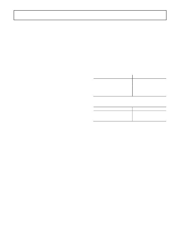
�pad� (EP)� of� the� package� are� soldered� on� the� PCB.� Table� 6� shows�
�typical� θ� JA� values� for� the� 16-lead� LFCSP� for� various� PCB� copper�
�sizes.� Table� 7� shows� typical� Ψ� JB� values� for� the� 16-lead� LFCSP.�
�Table� 6.� Typical� θ� JA� Values�
�Copper� Size� (mm� 2� )� θ� JA� (°C/W),� LFCSP�
�The� ADP1740/ADP1741� have� an� internal� undervoltage� lockout�
�circuit� that� disables� all� inputs� and� the� output� when� the� input�
�voltage� is� less� than� approximately� 1.58� V.� This� ensures� that� the�
�ADP1740/ADP1741� inputs� and� the� output� behave� in� a� predict-�
�able� manner� during� power-up.�
�0� 1�
�100�
�500�
�1000�
�6400�
�130�
�80�
�69�
�54�
�42�
�Device� soldered� to� minimum� size� pin� traces.�
�CURRENT-LIMIT� AND� THERMAL� OVERLOAD�
�PROTECTION�
�The� ADP1740/ADP1741� are� protected� against� damage� due� to�
�excessive� power� dissipation� by� current-limit� and� thermal�
�overload� protection� circuits.� The� ADP1740/ADP1741� are�
�designed� to� reach� current� limit� when� the� output� load� reaches�
�3� A� (typical).� When� the� output� load� exceeds� 3� A,� the� output�
�1�
�Table� 7.� Typical� Ψ� JB� Values�
�Copper� Size� (mm� 2� )� Ψ� JB� (°C/W)� @� 1� W�
�100� 32.7�
�500� 31.5�
�1000� 25.5�
�voltage� is� reduced� to� maintain� a� constant� current� limit.�
�Thermal� overload� protection� is� included,� which� limits� the�
�junction� temperature� to� a� maximum� of� 150°C� (typical).� Under�
�extreme� conditions� (that� is,� high� ambient� temperature� and� power�
�dissipation)� when� the� junction� temperature� begins� to� rise� above�
�150°C,� the� output� is� turned� off,� reducing� the� output� current� to�
�zero.� When� the� junction� temperature� drops� below� 135°C�
�The� junction� temperature� of� the� ADP1740/ADP1741� can� be�
�calculated� from� the� following� equation:�
�T� J� =� T� A� +� (� P� D� ×� θ� JA� )�
�where:�
�T� A� is� the� ambient� temperature.�
�P� D� is� the� power� dissipation� in� the� die,� given� by�
�(4)�
�(typical),� the� output� is� turned� on� again� and� output� current� is�
�restored� to� its� nominal� value.�
�Consider� the� case� where� a� hard� short� from� VOUT� to� ground�
�occurs.� At� first,� the� ADP1740/ADP1741� reach� current� limit� so�
�that� only� 3� A� is� conducted� into� the� short.� If� self-heating� of� the�
�junction� becomes� great� enough� to� cause� its� temperature� to� rise�
�above� 150°C,� thermal� shutdown� activates,� turning� off� the� output�
�and� reducing� the� output� current� to� zero.� As� the� junction� temper-�
�ature� cools� and� drops� below� 135°C,� the� output� turns� on� and�
�conducts� 3� A� into� the� short,� again� causing� the� junction� temper-�
�ature� to� rise� above� 150°C.� This� thermal� oscillation� between�
�135°C� and� 150°C� causes� a� current� oscillation� between� 3� A� and�
�0� A� that� continues� as� long� as� the� short� remains� at� the� output.�
�Current-limit� and� thermal� overload� protections� are� intended� to�
�protect� the� device� against� accidental� overload� conditions.� For�
�reliable� operation,� device� power� dissipation� should� be� externally�
�limited� so� that� junction� temperatures� do� not� exceed� 125°C.�
�P� D� =� [(� V� IN� ?� V� OUT� )� � I� LOAD� ]� +� (� V� IN� � I� GND� )� (5)�
�where:�
�V� IN� and� V� OUT� are� the� input� and� output� voltages,� respectively.�
�I� LOAD� is� the� load� current.�
�I� GND� is� the� ground� current.�
�Power� dissipation� due� to� ground� current� is� quite� small� and� can�
�be� ignored.� Therefore,� the� junction� temperature� equation� can�
�be� simplified� as� follows:�
�T� J� =� T� A� +� {[(� V� IN� ?� V� OUT� )� ×� I� LOAD� ]� ×� θ� JA� }� (6)�
�As� shown� in� Equation� 6,� for� a� given� ambient� temperature,� input-�
�to-output� voltage� differential,� and� continuous� load� current,� a�
�minimum� copper� size� requirement� exists� for� the� PCB� to� ensure�
��through� Figure� 41� show� junction� temperature� calculations� for�
�different� ambient� temperatures,� load� currents,� V� IN� to� V� OUT�
�differentials,� and� areas� of� PCB� copper.�
�Rev.� F� |� Page� 15� of� 20�
�相关PDF资料 |
PDF描述 |
|---|---|
| ADP1752ACPZ-1.8-R7 | IC REG LDO 1.8V .8A 16LFCSP |
| ADP1754ACPZ-1.2-R7 | IC REG LDO 1.2V 1.2A 16LFCSP |
| ADP1821ARQZ-R7 | IC REG CTRLR BUCK PWM VM 16-QSOP |
| ADP1822ARQZ-R7 | IC REG CTRLR BUCK PWM VM 24-QSOP |
| ADP1823ACPZ-R7 | IC REG CTRLR BUCK PWM VM 32LFCSP |
相关代理商/技术参数 |
参数描述 |
|---|---|
| ADP1740ACPZ-2.5-R7 | 功能描述:IC REG LDO 2.5V 2A 16LFCSP RoHS:是 类别:集成电路 (IC) >> PMIC - 稳压器 - 线性 系列:- 产品培训模块:MIC5365/66 Ultra-small LDO Regulators 标准包装:1 系列:- 稳压器拓扑结构:正,固定式 输出电压:3V 输入电压:最高 5.5V 电压 - 压降(标准):0.155V @ 150mA 稳压器数量:1 电流 - 输出:150mA 电流 - 限制(最小):200mA 工作温度:-40°C ~ 125°C 安装类型:表面贴装 封装/外壳:4-UDFN 裸露焊盘,4-TMLF? 供应商设备封装:4-TMLF?(1x1) 包装:Digi-Reel® 其它名称:576-3192-6 |
| ADP1740-BL1-EVZ | 制造商:Analog Devices 功能描述:Evaluation Board For Low Dropout Linear Regulator 制造商:Analog Devices 功能描述:BLANK ADISIMPOWER EVAL ADP1740 - Boxed Product (Development Kits) |
| ADP1741 | 制造商:AD 制造商全称:Analog Devices 功能描述:2 A, Low Dropout, CMOS Linear Regulator |
| ADP1741ACPZ-R7 | 功能描述:IC REG LDO ADJ 2A 16LFCSP RoHS:是 类别:集成电路 (IC) >> PMIC - 稳压器 - 线性 系列:- 产品培训模块:MIC5365/66 Ultra-small LDO Regulators 标准包装:1 系列:- 稳压器拓扑结构:正,固定式 输出电压:3V 输入电压:最高 5.5V 电压 - 压降(标准):0.155V @ 150mA 稳压器数量:1 电流 - 输出:150mA 电流 - 限制(最小):200mA 工作温度:-40°C ~ 125°C 安装类型:表面贴装 封装/外壳:4-UDFN 裸露焊盘,4-TMLF? 供应商设备封装:4-TMLF?(1x1) 包装:Digi-Reel® 其它名称:576-3192-6 |
| ADP1741-EVALZ | 功能描述:BOARD EVAL 2A ADP1741 RoHS:是 类别:编程器,开发系统 >> 评估板 - 线性稳压器 (LDO) 系列:- 产品变化通告:1Q2012 Discontinuation 30/Mar/2012 设计资源:NCP590MNDPTAGEVB Gerber Files 标准包装:1 系列:- 每 IC 通道数:2 - 双 输出电压:1.8V,2.8V 电流 - 输出:300mA 输入电压:2.1 ~ 5.5 V 稳压器类型:正,固定式 工作温度:-40°C ~ 85°C 板类型:完全填充 已供物品:板 已用 IC / 零件:NCP590MNDP 其它名称:NCP590MNDPTAGEVB-NDNCP590MNDPTAGEVBOS |
发布紧急采购,3分钟左右您将得到回复。