- 您现在的位置:买卖IC网 > PDF目录1776 > ADP1829ACPZ-R7 (Analog Devices Inc)IC REG CTRLR BUCK PWM VM 32LFCSP PDF资料下载
参数资料
| 型号: | ADP1829ACPZ-R7 |
| 厂商: | Analog Devices Inc |
| 文件页数: | 19/28页 |
| 文件大小: | 0K |
| 描述: | IC REG CTRLR BUCK PWM VM 32LFCSP |
| 标准包装: | 1 |
| PWM 型: | 电压模式 |
| 输出数: | 2 |
| 频率 - 最大: | 720kHz |
| 占空比: | 93% |
| 电源电压: | 3 V ~ 20 V |
| 降压: | 是 |
| 升压: | 无 |
| 回扫: | 无 |
| 反相: | 无 |
| 倍增器: | 无 |
| 除法器: | 无 |
| Cuk: | 无 |
| 隔离: | 无 |
| 工作温度: | -40°C ~ 125°C |
| 封装/外壳: | 32-VFQFN 裸露焊盘,CSP |
| 包装: | 标准包装 |
| 产品目录页面: | 791 (CN2011-ZH PDF) |
| 配用: | ADP1829-EVALZ-ND - BOARD EVALUATION ADP1829 |
| 其它名称: | ADP1829ACPZ-R7DKR |
第1页第2页第3页第4页第5页第6页第7页第8页第9页第10页第11页第12页第13页第14页第15页第16页第17页第18页当前第19页第20页第21页第22页第23页第24页第25页第26页第27页第28页
�� �
�
�Data� Sheet�
�COMPENSATING� THE� VOLTAGE� MODE� BUCK�
�LC� FILTER� BODE� PLOT�
�ADP1829�
�REGULATOR�
�Assuming� the� LC� filter� design� is� complete,� the� feedback� control�
�system� can� then� be� compensated.� Good� compensation� is� critical�
�to� proper� operation� of� the� regulator.� Calculate� the� quantities� in�
�GAIN�
�0dB�
�f� LC�
�–40dB/dec�
�f� ESR�
�f� CO�
�f� SW�
�FREQUENCY�
�Equation� 19� through� Equation� 47� to� derive� the� compensation�
�values.� The� goal� is� to� guarantee� that� the� voltage� gain� of� the� buck�
�converter� crosses� unity� at� a� slope� that� provides� adequate� phase�
�margin� for� stable� operation.� Additionally,� at� frequencies� above�
�the� crossover� frequency,� f� CO� ,� guaranteeing� sufficient� gain�
�margin� and� attenuation� of� switching� noise� are� important�
�secondary� goals.� For� initial� practical� designs,� a� good� choice� for�
�the� crossover� frequency� is� 1/10� of� the� switching� frequency,� so�
�first� calculate�
�PHASE�
�0°�
�–20dB/dec�
�A� FILTER�
�f� CO� ?�
�f� SW�
�10�
�(19)�
�This� gives� sufficient� frequency� range� to� design� a� compensation�
�that� attenuates� switching� artifacts,� while� also� giving� sufficient�
�control� loop� bandwidth� to� provide� good� transient� response.�
�The� output� LC� filter� is� a� resonant� network� that� inflicts� two� poles�
�upon� the� response� at� a� frequency� f� LC� ,� so� next� calculate�
�–90°�
�–180°�
�Φ� FILTER�
�f� LC� ?�
�1�
�2� π� LC�
�(20)�
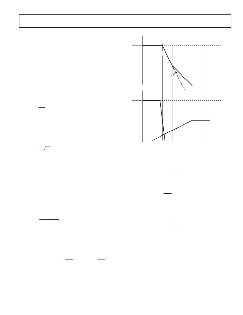
�Figure� 26.� LC� Filter� Bode� Plot�
�To� compensate� the� control� loop,� the� gain� of� the� system� must� be�
�Generally� speaking,� the� LC� corner� frequency� is� about� two�
�orders� of� magnitude� below� the� switching� frequency,� and�
�brought� back� up� so� that� it� is� 0� dB� at� the� desired� crossover�
�frequency.� Some� gain� is� provided� by� the� PWM� modulation� itself.�
�A� MOD� ?� 20� log� ?�
�?�
�?�
�therefore,� about� one� order� of� magnitude� below� crossover.� To�
�achieve� sufficient� phase� margin� at� crossover� to� guarantee�
�stability,� the� design� must� compensate� for� the� two� poles� at� the�
�?� V� IN�
�?�
�?� V� RAMP�
�?�
�?�
�(23)�
�?� V� IN�
�A� MOD� ?� 20� log� ?�
�?�
�?� 1� .� 3� V� ?�
�LC� corner� frequency� with� two� zeros� to� boost� the� system� phase�
�prior� to� crossover.� The� two� zeros� require� an� additional� pole� or�
�two� above� the� crossover� frequency� to� guarantee� adequate� gain�
�margin� and� attenuation� of� switching� noise� at� high� frequencies.�
�For� systems� using� the� internal� oscillator,� this� becomes�
�?�
�?� ?�
�(24)�
�Depending� on� component� selection,� one� zero� might� already� be�
�generated� by� the� equivalent� series� resistance� (ESR)� of� the� output�
�capacitor.� Calculate� this� zero� corner� frequency,� f� ESR� ,� as�
�Note� that� if� the� converter� is� being� synchronized,� the� ramp�
�voltage,� V� RAMP� ,� is� lower� than� 1.3� V� by� the� percentage� of�
�frequency� increase� over� the� nominal� setting� of� the� FREQ� pin.�
�f� ESR� ?�
�V� RAMP� ?� 1� .� 3� V� ?�
�?�
�?�
�1�
�2� π� R� ESR� C� OUT�
��(21)�
�?� 2� f� FREQ�
�?�
�?� f� SYNC�
�?�
�?�
�(25)�
�The� gain� of� the� LC� filter� at� crossover� can� be� linearly� approxi-�
�mated� from� Figure� 26� as�
�A� FILTER� ?� A� LC� ?� A� ESR�
�The� factor� of� 2� in� the� numerator� takes� into� account� that� the�
�SYNC� frequency� is� divided� by� 2� to� generate� the� switching�
�frequency.� For� example,� if� the� FREQ� pin� is� set� high� for� the�
�600� kHz� range� and� a� 2� MHz� SYNC� signal� is� applied,� the� ramp�
�A� FILTER� ?� ?� 40� dB� ?� log� ?� ESR�
�?� ?� 20� dB� ?� log� ?� f� CO�
�?� f�
�?�
�?� ESR�
�?�
�?�
�?� f�
�?�
�?� f� LC�
�?� ?�
�?�
�?�
�?�
�(22)�
�voltage� is� 0.78� V.� This� increases� the� gain� of� the� modulator� by�
�4.4� dB� in� this� example.�
�If� f� ESR� ≈� f� CO� ,� then� add� another� 3� dB� to� account� for� the� local�
�difference� between� the� exact� solution� and� the� linear� approxima-�
�tion� in� Equation� 22.�
�Rev.� C� |� Page� 19� of� 28�
�相关PDF资料 |
PDF描述 |
|---|---|
| ADP1850ACPZ-R7 | IC REG CTRLR BUCK PWM CM 32LFCSP |
| ADP1864AUJZ-R7 | IC REG CTRLR BUCK PWM TSOT23-6 |
| ADP1871ACPZ-0.6-R7 | IC REG CTRLR BUCK PWM CM 10LFCSP |
| ADP1873ARMZ-0.3-R7 | IC REG CTRLR BUCK PWM CM 10-MSOP |
| ADP1875ARQZ-0.3-R7 | IC REG CTRLR BUCK PWM CM 16-QSOP |
相关代理商/技术参数 |
参数描述 |
|---|---|
| ADP1829-BL1-EVZ | 制造商:Analog Devices 功能描述:BLANK ADISIMPOWER EVAL ADP1829 - Boxed Product (Development Kits) |
| ADP1829-BL2-EVZ | 制造商:Analog Devices 功能描述:Evaluation Board For Dual Interleaved Step-Down DC-To-DC Controller With Tracking 制造商:Analog Devices 功能描述:BLANK ADISIMPOWER EVAL ADP1829 - Boxed Product (Development Kits) |
| ADP1829-EVALZ | 功能描述:BOARD EVALUATION ADP1829 RoHS:是 类别:编程器,开发系统 >> 评估板 - DC/DC 与 AC/DC(离线)SMPS 系列:- 产品培训模块:Obsolescence Mitigation Program 标准包装:1 系列:True Shutdown™ 主要目的:DC/DC,步升 输出及类型:1,非隔离 功率 - 输出:- 输出电压:- 电流 - 输出:1A 输入电压:2.5 V ~ 5.5 V 稳压器拓扑结构:升压 频率 - 开关:3MHz 板类型:完全填充 已供物品:板 已用 IC / 零件:MAX8969 |
| ADP1850 | 制造商:AD 制造商全称:Analog Devices 功能描述:Wide Range Input, Dual/Two-Phase, DC-to-DC Synchronous Buck Controller |
| ADP1850ACPZ | 制造商:Analog Devices 功能描述:IC BUCK CNTRL SYNC 2PH 32LFCSP |
发布紧急采购,3分钟左右您将得到回复。