- 您现在的位置:买卖IC网 > PDF目录17393 > ADP1874-0.6-EVALZ (Analog Devices Inc)BOARD EVAL FOR ADP1874 PDF资料下载
参数资料
| 型号: | ADP1874-0.6-EVALZ |
| 厂商: | Analog Devices Inc |
| 文件页数: | 20/44页 |
| 文件大小: | 0K |
| 描述: | BOARD EVAL FOR ADP1874 |
| 标准包装: | 1 |
| 系列: | * |
第1页第2页第3页第4页第5页第6页第7页第8页第9页第10页第11页第12页第13页第14页第15页第16页第17页第18页第19页当前第20页第21页第22页第23页第24页第25页第26页第27页第28页第29页第30页第31页第32页第33页第34页第35页第36页第37页第38页第39页第40页第41页第42页第43页第44页
�� �
�
�ADP1874/ADP1875�
�ON-BOARD� LOW� DROPOUT� REGULATOR�
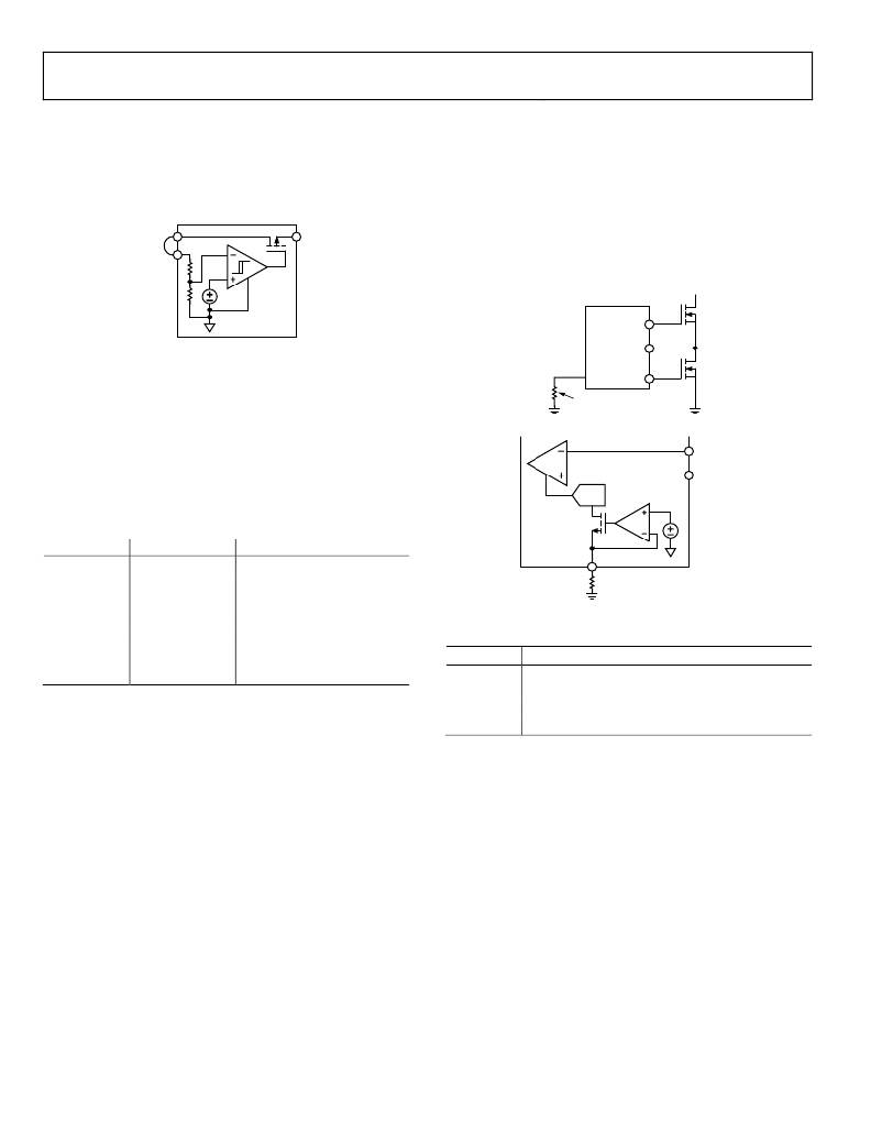
�The� ADP1874� /� ADP1875� use� an� on-board� LDO� to� bias� the�
�internal� digital� and� analog� circuitry.� Connect� the� VREG� and�
�VREG_IN� pins� together� for� normal� LDO� operation� for� low�
��ON-BOARD� REGULATOR�
�Data� Sheet�
�The� RES� detect� circuit� digitizes� the� value� of� the� resistor� at� the�
�RES� pin� (Pin� 6).� An� internal� ADC� outputs� a� 2-bit� digital� code�
�that� is� used� to� program� four� separate� gain� configurations� in� the�
�current-sense� amplifier� (see� Figure� 69).� Each� configuration� corre-�
�sponds� to� a� current-sense� gain� (A� CS� )� of� 3� V/V,� 6� V/V,� 12� V/V,� or�
�24� V/V,� respectively� (see� Table� 6� and� Table� 7).� This� variable� is� used�
�VREG�
�VREG_IN�
�REF�
�VIN�
�for� the� valley� current-limit� setting,� which� sets� up� the� appropriate�
�current-sense� gain� for� a� given� application� and� sets� the� compensation�
�necessary� to� achieve� loop� stability� (see� the� Valley� Current-Limit�
�Setting� section� and� the� Compensation� Network� section).�
�Q1�
�DRVH�
�Figure� 67.� Connecting� VREG� and� VREG_IN� Together�
�SW�
�With� proper� bypass� capacitors� connected� to� the� VREG� pin� (output�
�of� the� internal� LDO),� this� pin� also� provides� power� for� the� internal�
�MOSFET� drivers.� It� is� recommended� to� float� VREG/VREG_IN�
�RES�
�DRVL�
�CS� GAIN�
�PROGRAMMING�
�Q2�
�if� VIN� is� used� for� greater� than� 5.5� V� operation.� The� minimum�
�Figure� 68.� Programming� Resistor� Location�
�voltage� where� bias� is� guaranteed� to� operate� is� 2.75� V� at� VREG.�
�For� applications� where� VIN� is� decoupled� from� VREG,� the�
�minimum� voltage� at� VIN� must� be� 2.9� V.� It� is� recommended� to� tie�
�CS�
�AMP�
�SW�
�PGND�
�VIN� and� VREG� together� if� the� VIN� pin� is� subjected� to� a� 2.75� V� rail.�
�CS� GAIN�
�SET�
�ADC�
�0.4V�
�Table� 5.� Power� Input� and� LDO� Output� Configurations�
�VIN�
�>5.5� V�
�VREG/VREG_IN�
�Float�
�Comments�
�Must� use� the� LDO.�
�<5.5� V�
�<5.5� V�
�VIN� Ranging�
�Above� and�
�Below� 5.5� V�
�Connect� to� VIN�
�Float�
�Float�
�LDO� drop� voltage� is� not�
�realized� (that� is,� if� VIN� =� 2.75� V,�
�then� VREG� =� 2.75� V).�
�LDO� drop� is� realized.�
�LDO� drop� is� realized,�
�minimum� VIN�
�recommendation� is� 2.95� V.�
�RES�
�Figure� 69.� RES� Detect� Circuit� for� Current-Sense� Gain� Programming�
�Table� 6.� Current-Sense� Gain� Programming�
�Resistor� A� CS�
�47� k� 3� V/V�
�THERMAL� SHUTDOWN�
�The� thermal� shutdown� is� a� self-protection� feature� to� prevent� the�
�22� k�
�Open�
�100� k�
�6� V/V�
�12� V/V�
�24� V/V�
�IC� from� damage� due� to� a� very� high� operating� junction� temperature.�
�If� the� junction� temperature� of� the� device� exceeds� 155°C,� the� part�
�enters� the� thermal� shutdown� state.� In� this� state,� the� device� shuts� off�
�both� the� upper� side� and� lower� side� MOSFETs� and� disables� the� entire�
�controller� immediately,� thus� reducing� the� power� consumption� of�
�the� IC.� The� part� resumes� operation� after� the� junction� temperature�
�of� the� part� cools� to� less� than� 140°C.�
�PROGRAMMING� RESISTOR� (RES)� DETECT� CIRCUIT�
�Upon� startup,� one� of� the� first� blocks� to� become� active� is� the� RES�
�detect� circuit.� This� block� powers� up� before� soft� start� begins.� It�
�forces� a� 0.4� V� reference� value� at� the� RES� pin� (see� Figure� 68)� and� is�
�programmed� to� identify� four� possible� resistor� values:� 47� k?,� 22� k?,�
�open,� and� 100� k?.�
�VALLEY� CURRENT-LIMIT� SETTING�
�The� architecture� of� the� ADP1874� /� ADP1875� is� based� on� valley�
�current-mode� control.� The� current� limit� is� determined� by� three�
�components:� the� R� ON� of� the� lower� side� MOSFET,� the� current-�
�sense� amplifier� output� voltage� swing,� and� the� current-sense� gain.�
�The� CS� output� voltage� range� is� internally� fixed� at� 1.4� V.� The�
�current-sense� gain� is� programmable� via� an� external� resistor� at�
��section).� The� R� ON� of� the� lower� side� MOSFET� can� vary� over�
�temperature� and� usually� has� a� positive� T� C� (meaning� that� it�
�increases� with� temperature);� therefore,� it� is� recommended� to�
�program� the� current-sense� gain� resistor� based� on� the� rated� R� ON�
�of� the� MOSFET� at� 125°C.�
�Rev.� A� |� Page� 20� of� 44�
�相关PDF资料 |
PDF描述 |
|---|---|
| A9AAT-0704E | FLEX CABLE - AFH07T/AE07/AFH07T |
| ADP1875-1.0-EVALZ | BOARD EVAL 1MHZ ADP1875 |
| GBC28DRTS-S13 | CONN EDGECARD 56POS .100 EXTEND |
| EBC30DRTS-S13 | CONN EDGECARD 60POS .100 EXTEND |
| A9AAT-0208F | FLEX CABLE - AFE02T/AF02/AFE02T |
相关代理商/技术参数 |
参数描述 |
|---|---|
| ADP1874-1.0-EVALZ | 功能描述:BOARD EVAL FOR ADP1874 RoHS:是 类别:编程器,开发系统 >> 评估板 - DC/DC 与 AC/DC(离线)SMPS 系列:* 产品培训模块:Obsolescence Mitigation Program 标准包装:1 系列:True Shutdown™ 主要目的:DC/DC,步升 输出及类型:1,非隔离 功率 - 输出:- 输出电压:- 电流 - 输出:1A 输入电压:2.5 V ~ 5.5 V 稳压器拓扑结构:升压 频率 - 开关:3MHz 板类型:完全填充 已供物品:板 已用 IC / 零件:MAX8969 |
| ADP1874ARQZ-0.3-R7 | 功能描述:IC REG CTRLR BUCK PWM CM 16-QSOP RoHS:是 类别:集成电路 (IC) >> PMIC - 稳压器 - DC DC 切换控制器 系列:- 特色产品:LM3753/54 Scalable 2-Phase Synchronous Buck Controllers 标准包装:1 系列:PowerWise® PWM 型:电压模式 输出数:1 频率 - 最大:1MHz 占空比:81% 电源电压:4.5 V ~ 18 V 降压:是 升压:无 回扫:无 反相:无 倍增器:无 除法器:无 Cuk:无 隔离:无 工作温度:-5°C ~ 125°C 封装/外壳:32-WFQFN 裸露焊盘 包装:Digi-Reel® 产品目录页面:1303 (CN2011-ZH PDF) 其它名称:LM3754SQDKR |
| ADP1874ARQZ-0.6-R7 | 功能描述:IC REG CTRLR BUCK PWM CM 16-QSOP RoHS:是 类别:集成电路 (IC) >> PMIC - 稳压器 - DC DC 切换控制器 系列:- 标准包装:2,500 系列:- PWM 型:电流模式 输出数:1 频率 - 最大:500kHz 占空比:96% 电源电压:4 V ~ 36 V 降压:无 升压:是 回扫:无 反相:无 倍增器:无 除法器:无 Cuk:无 隔离:无 工作温度:-40°C ~ 125°C 封装/外壳:24-WQFN 裸露焊盘 包装:带卷 (TR) |
| ADP1874ARQZ-1.0-R7 | 功能描述:IC REG CTRLR BUCK PWM CM 16-QSOP RoHS:是 类别:集成电路 (IC) >> PMIC - 稳压器 - DC DC 切换控制器 系列:- 标准包装:2,500 系列:- PWM 型:电流模式 输出数:1 频率 - 最大:500kHz 占空比:96% 电源电压:4 V ~ 36 V 降压:无 升压:是 回扫:无 反相:无 倍增器:无 除法器:无 Cuk:无 隔离:无 工作温度:-40°C ~ 125°C 封装/外壳:24-WQFN 裸露焊盘 包装:带卷 (TR) |
| ADP1875 | 制造商:AD 制造商全称:Analog Devices 功能描述:Synchronous Buck Controller with Constant On-Time and Valley Current Mode |
发布紧急采购,3分钟左右您将得到回复。