- 您现在的位置:买卖IC网 > PDF目录17393 > ADP1874-0.6-EVALZ (Analog Devices Inc)BOARD EVAL FOR ADP1874 PDF资料下载
参数资料
| 型号: | ADP1874-0.6-EVALZ |
| 厂商: | Analog Devices Inc |
| 文件页数: | 38/44页 |
| 文件大小: | 0K |
| 描述: | BOARD EVAL FOR ADP1874 |
| 标准包装: | 1 |
| 系列: | * |
第1页第2页第3页第4页第5页第6页第7页第8页第9页第10页第11页第12页第13页第14页第15页第16页第17页第18页第19页第20页第21页第22页第23页第24页第25页第26页第27页第28页第29页第30页第31页第32页第33页第34页第35页第36页第37页当前第38页第39页第40页第41页第42页第43页第44页
�� �
�
�ADP1874/ADP1875�
�BOTTOM�
�RESISTOR� TAP�
�TO� ANALOG�
�GROUND� PLANE�
�PGND� SENSE� TAP� FROM�
�NEGATIVE� TERMINALS� OF�
�THE� OUTPUT� BULK�
�CAPACITORS.� THIS�
�TRACK� PLACEMENT�
�SHOULD� BE� DIRECTLY�
�BELOW� THE� VOUT� SENSE�
�LINE� OF� LAYER� 3.�
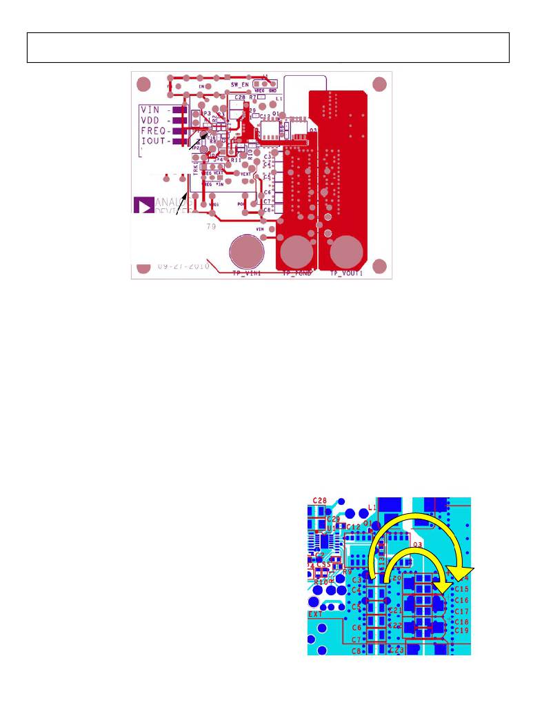
�Figure� 94.� Layer� 4� (Bottom� Layer)� of� ADP1874� /� ADP1875� Evaluation� Board�
�Data� Sheet�
�IC� SECTION� (LEFT� SIDE� OF� EVALUATION� BOARD)�
�A� dedicated� plane� for� the� analog� ground� plane� (GND)� should�
�be� separate� from� the� main� power� ground� plane� (PGND).� With�
�the� shortest� path� possible,� connect� the� analog� ground� plane� to�
�the� GND� pin� (Pin� 5).� This� plane� should� be� on� only� the� top� layer�
�of� the� evaluation� board.� To� avoid� crosstalk� interference,� there�
�should� not� be� any� other� voltage� or� current� pathway� directly� below�
�this� plane� on� Layer� 2,� Layer� 3,� or� Layer� 4.� Connect� the� negative�
�terminals� of� all� sensitive� analog� components� to� the� analog� ground�
�plane.� Examples� of� such� sensitive� analog� components� include�
�the� resistor� divider’s� bottom� resistor,� the� high� frequency� bypass�
�capacitor� for� biasing� (0.1� μF),� and� the� compensation� network.�
�Mount� a� 1� μF� bypass� capacitor� directly� across� the� VREG� pin�
�(Pin� 7)� and� the� PGND� pin� (Pin� 13).� In� addition,� a� 0.1� μF� should�
�be� tied� across� the� VREG� pin� (Pin� 7)� and� the� GND� pin� (Pin� 5).�
�POWER� SECTION�
�As� shown� in� Figure� 91,� an� appropriate� configuration� to� localize�
�large� current� transfer� from� the� high� voltage� input� (V� IN� )� to� the�
�output� (V� OUT� )� and� then� back� to� the� power� ground� is� to� put� the�
�V� IN� plane� on� the� left,� the� output� plane� on� the� right,� and� the� main�
�power� ground� plane� in� between� the� two.� Current� transfers� from�
�the� input� capacitors� to� the� output� capacitors,� through� Q1/Q2,�
�during� the� on� state� (see� Figure� 95).� The� direction� of� this� current�
�(yellow� arrow)� is� maintained� as� Q1/Q2� turns� off� and� Q3/Q4� turns�
�on.� When� Q3/Q4� turns� on,� the� current� direction� continues� to� be�
�maintained� (yellow� arrow)� as� it� circles� from� the� bulk� capacitor�
�power� ground� terminal� to� the� output� capacitors,� through�
�Q3/Q4.� Arranging� the� power� planes� in� this� manner� minimizes�
�the� area� in� which� changes� in� flux� occur� if� the� current� through�
�Q1/Q2� stops� abruptly.� Sudden� changes� in� flux,� usually� at� the�
�source� terminals� of� Q1/Q2� and� the� drain� terminal� of� Q3/Q4,�
�cause� large� dv/dt� at� the� SW� node.�
�The� SW� node� is� near� the� top� of� the� evaluation� board.� The� SW�
�node� should� use� the� least� amount� of� area� possible� and� be� away�
�from� any� sensitive� analog� circuitry� and� components.� This� is�
�because� the� SW� node� is� where� most� sudden� changes� in� flux�
�density� occur.� When� possible,� replicate� this� pad� onto� Layer� 2�
�and� Layer� 3� for� thermal� relief� and� eliminate� any� other� voltage� and�
�current� pathways� directly� beneath� the� SW� node� plane.� Populate�
�the� SW� node� plane� with� vias,� mainly� around� the� exposed� pad� of�
�the� inductor� terminal� and� around� the� perimeter� of� the� source� of�
�Q1/Q2� and� the� drain� of� Q3/Q4.� The� output� voltage� power� plane�
�(V� OUT� )� is� at� the� rightmost� end� of� the� evaluation� board.� This� plane�
�should� be� replicated,� descending� down� to� multiple� layers� with�
�vias� surrounding� the� inductor� terminal� and� the� positive� terminals�
�of� the� output� bulk� capacitors.� Ensure� that� the� negative� terminals� of�
�the� output� capacitors� are� placed� close� to� the� main� power� ground�
�(PGND),� as� previously� mentioned.� All� of� these� points� form� a�
�tight� circle� (component� geometry� permitting)� that� minimizes�
�the� area� of� flux� change� as� the� event� switches� between� D� and� 1� ?� D.�
�Figure� 95.� Primary� Current� Pathways� During� the� On� State� of� the� Upper� Side�
�MOSFET� (Left� Arrow)� and� the� On� State� of� the� Lower� Side� MOSFET� (Right� Arrow)�
�Rev.� A� |� Page� 38� of� 44�
�相关PDF资料 |
PDF描述 |
|---|---|
| A9AAT-0704E | FLEX CABLE - AFH07T/AE07/AFH07T |
| ADP1875-1.0-EVALZ | BOARD EVAL 1MHZ ADP1875 |
| GBC28DRTS-S13 | CONN EDGECARD 56POS .100 EXTEND |
| EBC30DRTS-S13 | CONN EDGECARD 60POS .100 EXTEND |
| A9AAT-0208F | FLEX CABLE - AFE02T/AF02/AFE02T |
相关代理商/技术参数 |
参数描述 |
|---|---|
| ADP1874-1.0-EVALZ | 功能描述:BOARD EVAL FOR ADP1874 RoHS:是 类别:编程器,开发系统 >> 评估板 - DC/DC 与 AC/DC(离线)SMPS 系列:* 产品培训模块:Obsolescence Mitigation Program 标准包装:1 系列:True Shutdown™ 主要目的:DC/DC,步升 输出及类型:1,非隔离 功率 - 输出:- 输出电压:- 电流 - 输出:1A 输入电压:2.5 V ~ 5.5 V 稳压器拓扑结构:升压 频率 - 开关:3MHz 板类型:完全填充 已供物品:板 已用 IC / 零件:MAX8969 |
| ADP1874ARQZ-0.3-R7 | 功能描述:IC REG CTRLR BUCK PWM CM 16-QSOP RoHS:是 类别:集成电路 (IC) >> PMIC - 稳压器 - DC DC 切换控制器 系列:- 特色产品:LM3753/54 Scalable 2-Phase Synchronous Buck Controllers 标准包装:1 系列:PowerWise® PWM 型:电压模式 输出数:1 频率 - 最大:1MHz 占空比:81% 电源电压:4.5 V ~ 18 V 降压:是 升压:无 回扫:无 反相:无 倍增器:无 除法器:无 Cuk:无 隔离:无 工作温度:-5°C ~ 125°C 封装/外壳:32-WFQFN 裸露焊盘 包装:Digi-Reel® 产品目录页面:1303 (CN2011-ZH PDF) 其它名称:LM3754SQDKR |
| ADP1874ARQZ-0.6-R7 | 功能描述:IC REG CTRLR BUCK PWM CM 16-QSOP RoHS:是 类别:集成电路 (IC) >> PMIC - 稳压器 - DC DC 切换控制器 系列:- 标准包装:2,500 系列:- PWM 型:电流模式 输出数:1 频率 - 最大:500kHz 占空比:96% 电源电压:4 V ~ 36 V 降压:无 升压:是 回扫:无 反相:无 倍增器:无 除法器:无 Cuk:无 隔离:无 工作温度:-40°C ~ 125°C 封装/外壳:24-WQFN 裸露焊盘 包装:带卷 (TR) |
| ADP1874ARQZ-1.0-R7 | 功能描述:IC REG CTRLR BUCK PWM CM 16-QSOP RoHS:是 类别:集成电路 (IC) >> PMIC - 稳压器 - DC DC 切换控制器 系列:- 标准包装:2,500 系列:- PWM 型:电流模式 输出数:1 频率 - 最大:500kHz 占空比:96% 电源电压:4 V ~ 36 V 降压:无 升压:是 回扫:无 反相:无 倍增器:无 除法器:无 Cuk:无 隔离:无 工作温度:-40°C ~ 125°C 封装/外壳:24-WQFN 裸露焊盘 包装:带卷 (TR) |
| ADP1875 | 制造商:AD 制造商全称:Analog Devices 功能描述:Synchronous Buck Controller with Constant On-Time and Valley Current Mode |
发布紧急采购,3分钟左右您将得到回复。