- 您现在的位置:买卖IC网 > PDF目录17393 > ADP1874-0.6-EVALZ (Analog Devices Inc)BOARD EVAL FOR ADP1874 PDF资料下载
参数资料
| 型号: | ADP1874-0.6-EVALZ |
| 厂商: | Analog Devices Inc |
| 文件页数: | 24/44页 |
| 文件大小: | 0K |
| 描述: | BOARD EVAL FOR ADP1874 |
| 标准包装: | 1 |
| 系列: | * |
第1页第2页第3页第4页第5页第6页第7页第8页第9页第10页第11页第12页第13页第14页第15页第16页第17页第18页第19页第20页第21页第22页第23页当前第24页第25页第26页第27页第28页第29页第30页第31页第32页第33页第34页第35页第36页第37页第38页第39页第40页第41页第42页第43页第44页
�� �
�
�ADP1874/ADP1875�
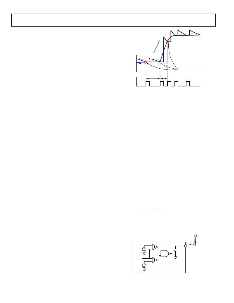
�PSEUDO-FIXED� FREQUENCY�
�The� ADP1874� /� ADP1875� employ� a� constant� on-time� control�
�scheme.� During� steady� state� operation,� the� switching� frequency�
�stays� relatively� constant,� or� pseudo-fixed.� This� is� due� to� the� one-�
�shot� t� ON� timer� that� produces� a� high-side� PWM� pulse� with� a� fixed�
�duration,� given� that� external� conditions� such� as� input� voltage,�
�output� voltage,� and� load� current� are� also� at� steady� state.� During�
�LOAD� CURRENT�
�DEMAND�
�CS� AMP�
�OUTPUT�
�Data� Sheet�
�load� transients,� the� frequency� momentarily� changes� for� the�
�duration� of� the� transient� event� so� that� the� output� comes� back�
�ERROR� AMP�
�OUTPUT�
�VALLEY�
�TRIP� POINTS�
�within� regulation� more� quickly� than� if� the� frequency� were� fixed�
�or� if� it� were� to� remain� unchanged.� After� the� transient� event� is�
�PWM� OUTPUT�
�f� SW�
�>� f� SW�
�complete,� the� frequency� returns� to� a� pseudo-fixed� value.�
�To� illustrate� this� feature� more� clearly,� this� section� describes�
�one� such� load� transient� event—a� positive� load� step—in� detail.�
�During� load� transient� events,� the� high-side� driver� output� pulse-�
�width� stays� relatively� consistent� from� cycle� to� cycle;� however,�
�the� off-time� (DRVL� on-time)� dynamically� adjusts� according� to�
�the� instantaneous� changes� in� the� external� conditions� mentioned.�
�When� a� positive� load� step� occurs,� the� error� amplifier� (out� of� phase�
�with� the� output,� V� OUT� )� produces� new� voltage� information� at� its�
�output� (COMP).� In� addition,� the� current-sense� amplifier� senses�
�new� inductor� current� information� during� this� positive� load�
�transient� event.� The� error� amplifier’s� output� voltage� reaction� is�
�compared� with� the� new� inductor� current� information� that� sets�
�the� start� of� the� next� switching� cycle.� Because� current� information�
�is� produced� from� valley� current� sensing,� it� is� sensed� at� the� down�
�ramp� of� the� inductor� current,� whereas� the� voltage� loop� information�
�is� sensed� through� the� counter� action� upswing� of� the� error�
�amplifier’s� output� (COMP).�
��which� allows� an� instantaneous� increase� in� switching� frequency�
�during� the� positive� load� transient� event.� In� summary,� a� positive�
�load� step� causes� V� OUT� to� transient� down,� which� causes� COMP� to�
�transient� up� and,� therefore,� shortens� the� off� time.� This� resulting�
�increase� in� frequency� during� a� positive� load� transient� helps� to�
�Figure� 78.� Load� Transient� Response� Operation�
�POWER� GOOD� MONITORING�
�The� ADP1874� /� ADP1875� power� good� circuitry� monitors� the�
�output� voltage� via� the� FB� pin.� The� PGOOD� pin� is� an� open-drain�
�output� that� can� be� pulled� up� by� an� external� resistor� to� a� voltage�
�rail� that� does� not� necessarily� have� to� be� VREG.� When� the� internal�
�NMOS� switch� is� in� high� impedance� (off� state),� this� means� that�
�the� PGOOD� pin� is� logic� high,� and� the� output� voltage� via� the� FB�
�pin� is� within� the� specified� regulation� window.� When� the� internal�
�switch� is� turned� on,� PGOOD� is� internally� pulled� low� when� the�
�output� voltage� via� the� FB� pin� is� outside� this� regulation� window.�
�The� power� good� window� is� defined� with� a� typical� upper�
�specification� of� +90� mV� and� a� lower� specification� of� ?70� mV�
�below� the� FB� voltage� of� 600� mV.� When� an� overvoltage� event� occurs�
�at� the� output,� there� is� a� typical� propagation� delay� of� 12� μs� prior�
�to� the� PGOOD� pin� deassertion� (logic� low).� When� the� output�
�voltage� re-enters� the� regulation� window,� there� is� a� propagation�
�delay� of� 12� μs� prior� to� PGOOD� reasserting� back� to� a� logic� high�
�state.� When� the� output� is� outside� the� regulation� window,� the�
�PGOOD� open� drain� switch� is� capable� of� sinking� 1mA� of� current�
�and� provides� 140� mV� of� drop� across� this� switch.� The� user� is� free�
�to� tie� the� external� pull-up� resistor� (R� RES� )� to� any� voltage� rail� up� to�
�20� V.� The� following� equation� provides� the� proper� external� pull-up�
�R� PGD� =� EXT�
�quickly� bring� V� OUT� back� up� in� value� and� within� the� regulation�
�window.�
�Similarly,� a� negative� load� step� causes� the� off� time� to� lengthen� in�
�resistor� value:�
�V�
�?� 140� mV�
�1� mA�
�response� to� V� OUT� rising.� This� effectively� increases� the� inductor�
�demagnetizing� phase,� helping� to� bring� V� OUT� within� regulation.�
�In� this� case,� the� switching� frequency� decreases,� or� experiences� a�
�foldback,� to� help� facilitate� output� voltage� recovery.�
�Because� the� ADP1874� /� ADP1875� have� the� ability� to� respond� rapidly�
�where:�
�R� PGD� is� the� PGOOD� external� resistor.�
�V� EXT� is� a� user-chosen� voltage� rail.�
�V� EXT�
�to� sudden� changes� in� load� demand,� the� recovery� period� in� which�
�the� output� voltage� settles� back� to� its� original� steady� state� operating�
�point� is� much� quicker� than� it� would� be� for� a� fixed-frequency�
�equivalent� .� Therefore,� using� a� pseudo-fixed� frequency� results� in�
�significantly� better� load-transient� performance� compared� to�
�690mV�
�FB�
�600mV�
�+�
�140mV�
�–�
�1mA�
�PGOOD�
�R� PGD�
�using� a� fixed� frequency.�
�Rev.� A� |� Page� 24� of� 44�
�530mV�
�Figure� 79.� Power� Good,� Output� Voltage� Monitoring� Circuit�
�相关PDF资料 |
PDF描述 |
|---|---|
| A9AAT-0704E | FLEX CABLE - AFH07T/AE07/AFH07T |
| ADP1875-1.0-EVALZ | BOARD EVAL 1MHZ ADP1875 |
| GBC28DRTS-S13 | CONN EDGECARD 56POS .100 EXTEND |
| EBC30DRTS-S13 | CONN EDGECARD 60POS .100 EXTEND |
| A9AAT-0208F | FLEX CABLE - AFE02T/AF02/AFE02T |
相关代理商/技术参数 |
参数描述 |
|---|---|
| ADP1874-1.0-EVALZ | 功能描述:BOARD EVAL FOR ADP1874 RoHS:是 类别:编程器,开发系统 >> 评估板 - DC/DC 与 AC/DC(离线)SMPS 系列:* 产品培训模块:Obsolescence Mitigation Program 标准包装:1 系列:True Shutdown™ 主要目的:DC/DC,步升 输出及类型:1,非隔离 功率 - 输出:- 输出电压:- 电流 - 输出:1A 输入电压:2.5 V ~ 5.5 V 稳压器拓扑结构:升压 频率 - 开关:3MHz 板类型:完全填充 已供物品:板 已用 IC / 零件:MAX8969 |
| ADP1874ARQZ-0.3-R7 | 功能描述:IC REG CTRLR BUCK PWM CM 16-QSOP RoHS:是 类别:集成电路 (IC) >> PMIC - 稳压器 - DC DC 切换控制器 系列:- 特色产品:LM3753/54 Scalable 2-Phase Synchronous Buck Controllers 标准包装:1 系列:PowerWise® PWM 型:电压模式 输出数:1 频率 - 最大:1MHz 占空比:81% 电源电压:4.5 V ~ 18 V 降压:是 升压:无 回扫:无 反相:无 倍增器:无 除法器:无 Cuk:无 隔离:无 工作温度:-5°C ~ 125°C 封装/外壳:32-WFQFN 裸露焊盘 包装:Digi-Reel® 产品目录页面:1303 (CN2011-ZH PDF) 其它名称:LM3754SQDKR |
| ADP1874ARQZ-0.6-R7 | 功能描述:IC REG CTRLR BUCK PWM CM 16-QSOP RoHS:是 类别:集成电路 (IC) >> PMIC - 稳压器 - DC DC 切换控制器 系列:- 标准包装:2,500 系列:- PWM 型:电流模式 输出数:1 频率 - 最大:500kHz 占空比:96% 电源电压:4 V ~ 36 V 降压:无 升压:是 回扫:无 反相:无 倍增器:无 除法器:无 Cuk:无 隔离:无 工作温度:-40°C ~ 125°C 封装/外壳:24-WQFN 裸露焊盘 包装:带卷 (TR) |
| ADP1874ARQZ-1.0-R7 | 功能描述:IC REG CTRLR BUCK PWM CM 16-QSOP RoHS:是 类别:集成电路 (IC) >> PMIC - 稳压器 - DC DC 切换控制器 系列:- 标准包装:2,500 系列:- PWM 型:电流模式 输出数:1 频率 - 最大:500kHz 占空比:96% 电源电压:4 V ~ 36 V 降压:无 升压:是 回扫:无 反相:无 倍增器:无 除法器:无 Cuk:无 隔离:无 工作温度:-40°C ~ 125°C 封装/外壳:24-WQFN 裸露焊盘 包装:带卷 (TR) |
| ADP1875 | 制造商:AD 制造商全称:Analog Devices 功能描述:Synchronous Buck Controller with Constant On-Time and Valley Current Mode |
发布紧急采购,3分钟左右您将得到回复。