- 您现在的位置:买卖IC网 > PDF目录17393 > ADP1874-0.6-EVALZ (Analog Devices Inc)BOARD EVAL FOR ADP1874 PDF资料下载
参数资料
| 型号: | ADP1874-0.6-EVALZ |
| 厂商: | Analog Devices Inc |
| 文件页数: | 30/44页 |
| 文件大小: | 0K |
| 描述: | BOARD EVAL FOR ADP1874 |
| 标准包装: | 1 |
| 系列: | * |
第1页第2页第3页第4页第5页第6页第7页第8页第9页第10页第11页第12页第13页第14页第15页第16页第17页第18页第19页第20页第21页第22页第23页第24页第25页第26页第27页第28页第29页当前第30页第31页第32页第33页第34页第35页第36页第37页第38页第39页第40页第41页第42页第43页第44页
�� �
�
�P� BODY� (� LOSS� )� =�
�� I� LOAD� � V� F� � 2�
�ADP1874/ADP1875�
�Diode� Conduction� Loss�
�The� ADP1874� /� ADP1875� employ� anti� cross-conduction� circuitry�
�that� prevents� the� upper� side� and� lower� side� MOSFETs� from�
�conducting� current� simultaneously.� This� overlap� control� is�
�beneficial,� avoiding� large� current� flow� that� may� lead� to� irreparable�
�damage� to� the� external� components� of� the� power� stage.� However,�
�this� blanking� period� comes� with� the� trade-off� of� a� diode�
�conduction� loss� occurring� immediately� after� the� MOSFET�
�change� states� and� continuing� well� into� idle� mode.� The� amount� of�
�loss� through� the� body� diode� of� the� lower� side� MOSFET� during�
�the� anti-overlap� state� is� given� by� the� following� expression:�
�t� BODY� (� LOSS� )�
�t� SW�
�where:�
�t� BODY(LOSS)� is� the� body� conduction� time� (see� Figure� 88� for� dead�
�time� periods).�
�t� SW� is� the� period� per� switching� cycle.�
�V� F� is� the� forward� drop� of� the� body� diode� during� conduction.�
�(See� the� selected� external� MOSFET� data� sheet� for� more�
�information� about� the� V� F� parameter.)�
�Data� Sheet�
�INPUT� CAPACITOR� SELECTION�
�The� goal� in� selecting� an� input� capacitor� is� to� reduce� or� minimize�
�input� voltage� ripple� and� to� reduce� the� high� frequency� source�
�impedance,� which� is� essential� for� achieving� predictable� loop�
�stability� and� transient� performance.�
�The� problem� with� using� bulk� capacitors,� other� than� their� physical�
�geometries,� is� their� large� equivalent� series� resistance� (ESR)� and�
�large� equivalent� series� inductance� (ESL).� Aluminum� electrolytic�
�capacitors� have� such� high� ESR� that� they� cause� undesired� input�
�voltage� ripple� magnitudes� and� are� generally� not� effective� at� high�
�switching� frequencies.�
�If� bulk� electrolytic� capacitors� are� used,� it� is� recommended� to� use�
�multilayered� ceramic� capacitors� (MLCC)� in� parallel� due� to� their�
�low� ESR� values.� This� dramatically� reduces� the� input� voltage� ripple�
�amplitude� as� long� as� the� MLCCs� are� mounted� directly� across� the�
�drain� of� the� upper� side� MOSFET� and� the� source� terminal� of� the�
�lower� side� MOSFET� (see� the� Layout� Considerations� section).�
�Improper� placement� and� mounting� of� these� MLCCs� may� cancel�
�their� effectiveness� due� to� stray� inductance� and� an� increase� in�
�trace� impedance.�
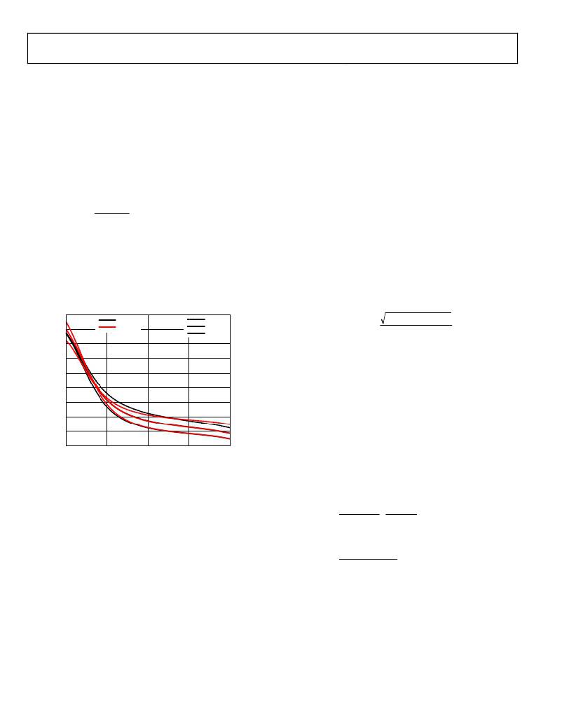
�80�
�72�
�1MHz�
�300kHz�
�+125°C�
�+25°C�
�–40°C�
�I� CIN� ,� RMS� =� I� LOAD� ,� MAX� �
�V� OUT� � (� V� IN� ?� V� OUT� )�
�V� OUT�
�C� IN,min� =�
�I� LOAD� ,� MAX� D� (� 1� ?� D� )�
�C� IN,min� =�
�64�
�56�
�48�
�40�
�32�
�24�
�16�
�8�
�2.7� 3.4� 4.1� 4.8� 5.5�
�VREG� (V)�
�Figure� 88.� Body� Diode� Conduction� Time� vs.� Low� Voltage� Input� (VREG)�
�Inductor� Loss�
�During� normal� conduction� mode,� further� power� loss� is� caused�
�by� the� conduction� of� current� through� the� inductor� windings,�
�which� have� dc� resistance� (DCR).� Typically,� larger� sized� inductors�
�have� smaller� DCR� values.�
�The� inductor� core� loss� is� a� result� of� the� eddy� currents� generated�
�within� the� core� material.� These� eddy� currents� are� induced� by� the�
�changing� flux,� which� is� produced� by� the� current� flowing� through�
�the� windings.� The� amount� of� inductor� core� loss� depends� on� the�
�The� maximum� input� voltage� ripple� and� maximum� input� capacitor�
�rms� current� occur� at� the� end� of� the� duration� of� 1� ?� D� while� the�
�upper� side� MOSFET� is� in� the� off� state.� The� input� capacitor� rms�
�current� reaches� its� maximum� at� Time� D.� When� calculating� the�
�maximum� input� voltage� ripple,� account� for� the� ESR� of� the� input�
�capacitor� as� follows:�
�V� MAX,RIPPLE� =� V� RIPP� +� (� I� LOAD,MAX� � ESR� )�
�where:�
�V� RIPP� is� usually� 1%� of� the� minimum� voltage� input.�
�I� LOAD,MAX� is� the� maximum� load� current.�
�ESR� is� the� equivalent� series� resistance� rating� of� the� input� capacitor.�
�Inserting� V� MAX,RIPPLE� into� the� charge� balance� equation� to�
�calculate� the� minimum� input� capacitor� requirement� gives�
��
�V� MAX� ,� RIPPLE� f� SW�
�or�
�I� LOAD� ,� MAX�
�4� f� SW� V� MAX� ,� RIPPLE�
�where� D� =� 50%.�
�P� DCR� (� LOSS� )� =� DCR� � I� LOAD� +� Core� Loss�
�core� material,� the� flux� swing,� the� frequency,� and� the� core� volume.�
�Ferrite� inductors� have� the� lowest� core� losses,� whereas� powdered� iron�
�inductors� have� higher� core� losses.� It� is� recommended� to� use� shielded�
��for� a� high� current,� dc-to-dc� switching� application� to� achieve�
�minimal� loss� and� negligible� electromagnetic� interference� (EMI).�
�2�
�Rev.� A� |� Page� 30� of� 44�
�相关PDF资料 |
PDF描述 |
|---|---|
| A9AAT-0704E | FLEX CABLE - AFH07T/AE07/AFH07T |
| ADP1875-1.0-EVALZ | BOARD EVAL 1MHZ ADP1875 |
| GBC28DRTS-S13 | CONN EDGECARD 56POS .100 EXTEND |
| EBC30DRTS-S13 | CONN EDGECARD 60POS .100 EXTEND |
| A9AAT-0208F | FLEX CABLE - AFE02T/AF02/AFE02T |
相关代理商/技术参数 |
参数描述 |
|---|---|
| ADP1874-1.0-EVALZ | 功能描述:BOARD EVAL FOR ADP1874 RoHS:是 类别:编程器,开发系统 >> 评估板 - DC/DC 与 AC/DC(离线)SMPS 系列:* 产品培训模块:Obsolescence Mitigation Program 标准包装:1 系列:True Shutdown™ 主要目的:DC/DC,步升 输出及类型:1,非隔离 功率 - 输出:- 输出电压:- 电流 - 输出:1A 输入电压:2.5 V ~ 5.5 V 稳压器拓扑结构:升压 频率 - 开关:3MHz 板类型:完全填充 已供物品:板 已用 IC / 零件:MAX8969 |
| ADP1874ARQZ-0.3-R7 | 功能描述:IC REG CTRLR BUCK PWM CM 16-QSOP RoHS:是 类别:集成电路 (IC) >> PMIC - 稳压器 - DC DC 切换控制器 系列:- 特色产品:LM3753/54 Scalable 2-Phase Synchronous Buck Controllers 标准包装:1 系列:PowerWise® PWM 型:电压模式 输出数:1 频率 - 最大:1MHz 占空比:81% 电源电压:4.5 V ~ 18 V 降压:是 升压:无 回扫:无 反相:无 倍增器:无 除法器:无 Cuk:无 隔离:无 工作温度:-5°C ~ 125°C 封装/外壳:32-WFQFN 裸露焊盘 包装:Digi-Reel® 产品目录页面:1303 (CN2011-ZH PDF) 其它名称:LM3754SQDKR |
| ADP1874ARQZ-0.6-R7 | 功能描述:IC REG CTRLR BUCK PWM CM 16-QSOP RoHS:是 类别:集成电路 (IC) >> PMIC - 稳压器 - DC DC 切换控制器 系列:- 标准包装:2,500 系列:- PWM 型:电流模式 输出数:1 频率 - 最大:500kHz 占空比:96% 电源电压:4 V ~ 36 V 降压:无 升压:是 回扫:无 反相:无 倍增器:无 除法器:无 Cuk:无 隔离:无 工作温度:-40°C ~ 125°C 封装/外壳:24-WQFN 裸露焊盘 包装:带卷 (TR) |
| ADP1874ARQZ-1.0-R7 | 功能描述:IC REG CTRLR BUCK PWM CM 16-QSOP RoHS:是 类别:集成电路 (IC) >> PMIC - 稳压器 - DC DC 切换控制器 系列:- 标准包装:2,500 系列:- PWM 型:电流模式 输出数:1 频率 - 最大:500kHz 占空比:96% 电源电压:4 V ~ 36 V 降压:无 升压:是 回扫:无 反相:无 倍增器:无 除法器:无 Cuk:无 隔离:无 工作温度:-40°C ~ 125°C 封装/外壳:24-WQFN 裸露焊盘 包装:带卷 (TR) |
| ADP1875 | 制造商:AD 制造商全称:Analog Devices 功能描述:Synchronous Buck Controller with Constant On-Time and Valley Current Mode |
发布紧急采购,3分钟左右您将得到回复。