- 您现在的位置:买卖IC网 > PDF目录17393 > ADP1874-0.6-EVALZ (Analog Devices Inc)BOARD EVAL FOR ADP1874 PDF资料下载
参数资料
| 型号: | ADP1874-0.6-EVALZ |
| 厂商: | Analog Devices Inc |
| 文件页数: | 29/44页 |
| 文件大小: | 0K |
| 描述: | BOARD EVAL FOR ADP1874 |
| 标准包装: | 1 |
| 系列: | * |
第1页第2页第3页第4页第5页第6页第7页第8页第9页第10页第11页第12页第13页第14页第15页第16页第17页第18页第19页第20页第21页第22页第23页第24页第25页第26页第27页第28页当前第29页第30页第31页第32页第33页第34页第35页第36页第37页第38页第39页第40页第41页第42页第43页第44页
�� �
�
�[�
�)� ]�
�DataSheet�
�EFFICIENCY� CONSIDERATION�
�One� of� the� important� criteria� to� consider� in� constructing� a� dc-to-dc�
�converter� is� efficiency.� By� definition,� efficiency� is� the� ratio� of� the�
�output� power� to� the� input� power.� For� high� power� applications� at�
�load� currents� up� to� 20� A,� the� following� are� important� MOSFET�
�parameters� that� aid� in� the� selection� process:�
�?� V� GS� (TH)� is� the� MOSFET� voltage� applied� between� the� gate�
�and� the� source� that� starts� channel� conduction.�
�?� R� DS� (ON)� is� the� MOSFET� on� resistance� during� channel�
�conduction.�
�?� Q� G� is� the� total� gate� charge.�
�?� C� N1� is� the� input� capacitance� of� the� upper� side� switch.�
�?� C� N2� is� the� input� capacitance� of� the� lower� side� switch.�
�The� following� are� the� losses� experienced� through� the� external�
�ADP1874/ADP1875�
�MOSFET� Driver� Loss�
�Other� dissipative� elements� are� the� MOSFET� drivers.� The� con-�
�tributing� factors� are� the� dc� current� flowing� through� a� driver�
�during� operation� and� the� Q� GATE� parameter� of� the� external� MOSFETs.�
�P� DR� (� LOSS� )� =� V� DR� � (� f� SW� C� upperFET� V� DR� +� I� BIAS� +�
�[� VREG� � (� f� SW� C� lowerFET� V� REG� +� I� BIAS� )� ]�
�where:�
�C� upperFET� is� the� input� gate� capacitance� of� the� upper� side� MOSFET.�
�C� lowerFET� is� the� input� gate� capacitance� of� the� lower� side� MOSFET.�
�I� BIAS� is� the� dc� current� flowing� into� the� upper� side� and� lower� side�
�drivers.�
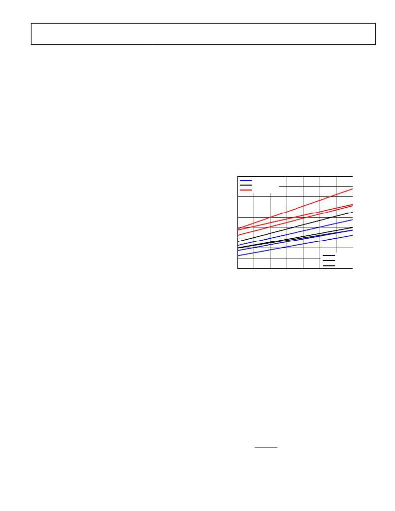
�V� DR� is� the� driver� bias� voltage� (that� is,� the� low� input� voltage�
�(� VREG� )� minus� the� rectifier� drop� (see� Figure� 87)).�
�VREG� is� the� bias� voltage.�
�component� during� normal� switching� operation:�
�800�
�VREG� =� 2.7V�
�?�
�?�
�?�
�?�
�?�
�Channel� conduction� loss� (both� the� MOSFETs)�
�MOSFET� driver� loss�
�MOSFET� switching� loss�
�Body� diode� conduction� loss� (lower� side� MOSFET)�
�Inductor� loss� (copper� and� core� loss)�
�720�
�640�
�560�
�480�
�VREG� =� 3.6V�
�VREG� =� 5.5V�
�+25°C�
�P� N1,N2(CL)� =� [� D� � R� N1(ON)� +� (� 1� ?� D� )� � R� N2(ON)� ]� � I� LOAD�
�Channel� Conduction� Loss�
�During� normal� operation,� the� bulk� of� the� loss� in� efficiency� is� due�
�to� the� power� dissipated� through� MOSFET� channel� conduction.�
�Power� loss� through� the� upper� side� MOSFET� is� directly� pro-�
�portional� to� the� duty-cycle� (D)� for� each� switching� period,� and�
�the� power� loss� through� the� lower� side� MOSFET� is� directly�
�proportional� to� 1� ?� D� for� each� switching� period.� The� selection�
�of� MOSFETs� is� governed� by� the� maximum� dc� load� current� that�
�the� converter� is� expected� to� deliver.� In� particular,� the� selection�
�of� the� lower� side� MOSFET� is� dictated� by� the� maximum� load�
�current� because� a� typical� high� current� application� employs� duty�
�cycles� of� less� than� 50%.� Therefore,� the� lower� side� MOSFET� is�
�in� the� on� state� for� most� of� the� switching� period.�
�2�
�400�
�320�
�240�
�+125°C�
�160�
�–40°C�
�80�
�300� 400� 500� 600� 700� 800� 900� 1000�
�SWITCHING� FREQUENCY� (kHz)�
�Figure� 87.� Internal� Rectifier� Voltage� Drop� vs.� Switching� Frequency�
�Switching� Loss�
�The� SW� node� transitions� due� to� the� switching� activities� of� the�
�upper� side� and� lower� side� MOSFETs.� This� causes� removal� and�
�replenishing� of� charge� to� and� from� the� gate� oxide� layer� of� the�
�MOSFET,� as� well� as� to� and� from� the� parasitic� capacitance�
�associated� with� the� gate� oxide� edge� overlap� and� the� drain� and�
�source� terminals.� The� current� that� enters� and� exits� these� charge�
�paths� presents� additional� loss� during� these� transition� times.�
�This� can� be� approximately� quantified� by� using� the� following�
�equation,� which� represents� the� time� in� which� charge� enters� and�
�exits� these� capacitive� regions:�
�t� SW-TRANS� =� R� GATE� � C� TOTAL�
�where:�
�C� TOTAL� is� the� C� GD� +� C� GS� of� the� external� MOSFET.�
�R� GATE� is� the� gate� input� resistance� of� the� external� MOSFET.�
�The� ratio� of� this� time� constant� to� the� period� of� one� switching� cycle�
�is� the� multiplying� factor� to� be� used� in� the� following� expression:�
�P� SW� (� LOSS� )� =�
�t� SW� -� TRANS�
�t� SW�
�� I� LOAD� � V� IN� � 2�
�or�
�P� SW(LOSS)� =� f� SW� � R� GATE� � C� TOTAL� � I� LOAD� � V� IN� � 2�
�Rev.� A� |� Page� 29� of� 44�
�相关PDF资料 |
PDF描述 |
|---|---|
| A9AAT-0704E | FLEX CABLE - AFH07T/AE07/AFH07T |
| ADP1875-1.0-EVALZ | BOARD EVAL 1MHZ ADP1875 |
| GBC28DRTS-S13 | CONN EDGECARD 56POS .100 EXTEND |
| EBC30DRTS-S13 | CONN EDGECARD 60POS .100 EXTEND |
| A9AAT-0208F | FLEX CABLE - AFE02T/AF02/AFE02T |
相关代理商/技术参数 |
参数描述 |
|---|---|
| ADP1874-1.0-EVALZ | 功能描述:BOARD EVAL FOR ADP1874 RoHS:是 类别:编程器,开发系统 >> 评估板 - DC/DC 与 AC/DC(离线)SMPS 系列:* 产品培训模块:Obsolescence Mitigation Program 标准包装:1 系列:True Shutdown™ 主要目的:DC/DC,步升 输出及类型:1,非隔离 功率 - 输出:- 输出电压:- 电流 - 输出:1A 输入电压:2.5 V ~ 5.5 V 稳压器拓扑结构:升压 频率 - 开关:3MHz 板类型:完全填充 已供物品:板 已用 IC / 零件:MAX8969 |
| ADP1874ARQZ-0.3-R7 | 功能描述:IC REG CTRLR BUCK PWM CM 16-QSOP RoHS:是 类别:集成电路 (IC) >> PMIC - 稳压器 - DC DC 切换控制器 系列:- 特色产品:LM3753/54 Scalable 2-Phase Synchronous Buck Controllers 标准包装:1 系列:PowerWise® PWM 型:电压模式 输出数:1 频率 - 最大:1MHz 占空比:81% 电源电压:4.5 V ~ 18 V 降压:是 升压:无 回扫:无 反相:无 倍增器:无 除法器:无 Cuk:无 隔离:无 工作温度:-5°C ~ 125°C 封装/外壳:32-WFQFN 裸露焊盘 包装:Digi-Reel® 产品目录页面:1303 (CN2011-ZH PDF) 其它名称:LM3754SQDKR |
| ADP1874ARQZ-0.6-R7 | 功能描述:IC REG CTRLR BUCK PWM CM 16-QSOP RoHS:是 类别:集成电路 (IC) >> PMIC - 稳压器 - DC DC 切换控制器 系列:- 标准包装:2,500 系列:- PWM 型:电流模式 输出数:1 频率 - 最大:500kHz 占空比:96% 电源电压:4 V ~ 36 V 降压:无 升压:是 回扫:无 反相:无 倍增器:无 除法器:无 Cuk:无 隔离:无 工作温度:-40°C ~ 125°C 封装/外壳:24-WQFN 裸露焊盘 包装:带卷 (TR) |
| ADP1874ARQZ-1.0-R7 | 功能描述:IC REG CTRLR BUCK PWM CM 16-QSOP RoHS:是 类别:集成电路 (IC) >> PMIC - 稳压器 - DC DC 切换控制器 系列:- 标准包装:2,500 系列:- PWM 型:电流模式 输出数:1 频率 - 最大:500kHz 占空比:96% 电源电压:4 V ~ 36 V 降压:无 升压:是 回扫:无 反相:无 倍增器:无 除法器:无 Cuk:无 隔离:无 工作温度:-40°C ~ 125°C 封装/外壳:24-WQFN 裸露焊盘 包装:带卷 (TR) |
| ADP1875 | 制造商:AD 制造商全称:Analog Devices 功能描述:Synchronous Buck Controller with Constant On-Time and Valley Current Mode |
发布紧急采购,3分钟左右您将得到回复。