- 您现在的位置:买卖IC网 > PDF目录10369 > ADS62C17IRGCR (Texas Instruments)IC ADC 11BIT SRL/PAR 200M 64VQFN PDF资料下载
参数资料
| 型号: | ADS62C17IRGCR |
| 厂商: | Texas Instruments |
| 文件页数: | 47/68页 |
| 文件大小: | 0K |
| 描述: | IC ADC 11BIT SRL/PAR 200M 64VQFN |
| 标准包装: | 2,000 |
| 位数: | 11 |
| 采样率(每秒): | 200M |
| 数据接口: | 串行,并联 |
| 转换器数目: | 2 |
| 功率耗散(最大): | 1.1W |
| 电压电源: | 模拟和数字 |
| 工作温度: | -40°C ~ 85°C |
| 安装类型: | 表面贴装 |
| 封装/外壳: | 64-VFQFN 裸露焊盘 |
| 供应商设备封装: | 64-VQFN 裸露焊盘(9x9) |
| 包装: | 带卷 (TR) |
| 输入数目和类型: | 2 个差分,单极 |
第1页第2页第3页第4页第5页第6页第7页第8页第9页第10页第11页第12页第13页第14页第15页第16页第17页第18页第19页第20页第21页第22页第23页第24页第25页第26页第27页第28页第29页第30页第31页第32页第33页第34页第35页第36页第37页第38页第39页第40页第41页第42页第43页第44页第45页第46页当前第47页第48页第49页第50页第51页第52页第53页第54页第55页第56页第57页第58页第59页第60页第61页第62页第63页第64页第65页第66页第67页第68页
CLKP
CLKM
VCM
0.1 F
m
0.1 F
m
CMOSclockinput
GAIN PROGRAMMABILITY
OFFSET CORRECTION
www.ti.com ............................................................................................................................................................. SLAS631A – APRIL 2009 – REVISED JULY 2009
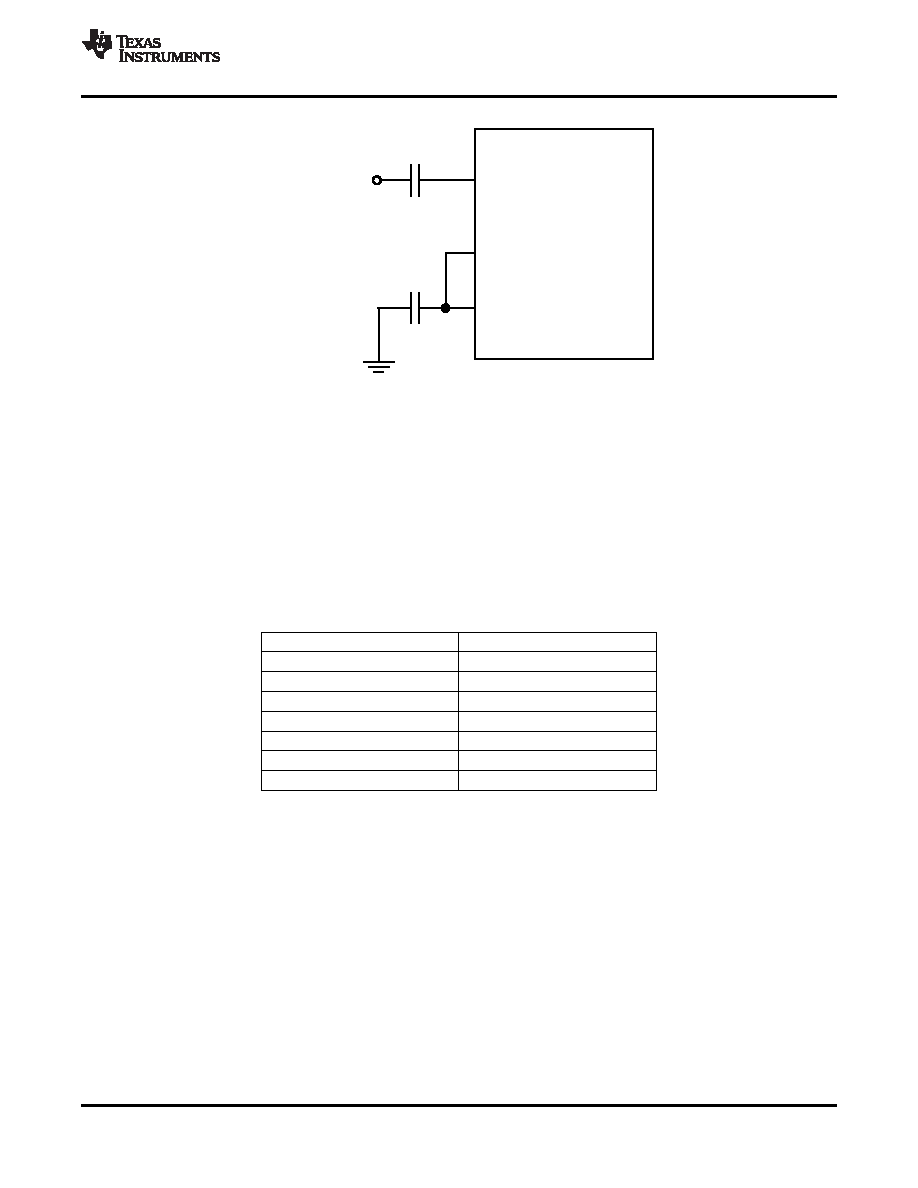
Figure 55. Single-Ended Clock Driving Circuit
ADS62C17 includes gain settings that can be used to get improved SFDR performance (compared to 0dB gain).
The gain is programmable from 0dB to 6dB (in 0.5 dB steps). For each gain setting, the analog input full-scale
range scales proportionally, as shown in Table 11.
The SFDR improvement is achieved at the expense of SNR; for each 1dB gain step, the SNR degrades about
1dB. The SNR degradation is less at high input frequencies. As a result, the gain is very useful at high input
frequencies as the SFDR improvement is significant with marginal degradation in SNR.
So, the gain can be used to trade-off between SFDR and SNR. Note that the default gain after reset is 0 dB.
Table 11. Full-Scale Range Across Gains
Gain, dB
Full-Scale, Vpp
0
2V
1
1.78
2
1.59
3
1.42
4
1.26
5
1.12
6
1.00
ADS62C17 has an internal offset correction algorithm that estimates and corrects dc offset up to +/-10mV. The
correction can be enabled using the serial register bit <OFFSET CORRECTION ENABLE>. Once enabled, the
algorithm estimates the channel offset and applies the correction every clock cycle. The time constant of the
correction loop is a function of the sampling clock frequency. The time constant can be controlled using register
bits <OFFSET CORR TIME CONSTANT> as described in Table 12.
After the offset is estimated, the correction can be frozen by setting <OFFSET CORRECTION ENABLE> = 0.
Once frozen, the last estimated value is used for offset correction every clock cycle. The correction does not
affect the phase of the signal. Note that offset correction is disabled by default after reset.
Figure 56 shows the time response of the offset correction algorithm, after it is enabled.
Copyright 2009, Texas Instruments Incorporated
51
Product Folder Link(s): ADS62C17
相关PDF资料 |
PDF描述 |
|---|---|
| D38999/20WG39BN | CONN HSG RCPT 39POS WALL MT SCKT |
| MS3106R22-23P | CONN PLUG 8POS STRAIGHT W/PINS |
| ISL54003IRTZ-T | IC AMP AUDIO PWR 1.23W AB 20TQFN |
| MS3101E24-9P | CONN RCPT 2POS FREE HNG W/PINS |
| CB3100R-18-11S | CONN RCPT 5POS WALL MNT W/SCKT |
相关代理商/技术参数 |
参数描述 |
|---|---|
| ADS62C17IRGCT | 功能描述:模数转换器 - ADC Dual Channel 11B 200MSPS ADC RoHS:否 制造商:Texas Instruments 通道数量:2 结构:Sigma-Delta 转换速率:125 SPs to 8 KSPs 分辨率:24 bit 输入类型:Differential 信噪比:107 dB 接口类型:SPI 工作电源电压:1.7 V to 3.6 V, 2.7 V to 5.25 V 最大工作温度:+ 85 C 安装风格:SMD/SMT 封装 / 箱体:VQFN-32 |
| ADS62P15 | 制造商:TI 制造商全称:Texas Instruments 功能描述:Dual Channel 11-Bits, 125 MSPS ADC With Parallel CMOS/DDR LVDS Outputs |
| ADS62P15_09 | 制造商:TI 制造商全称:Texas Instruments 功能描述:Dual Channel 11-Bits,125 MSPS ADC With Parallel CMOS/DDR LVDS Outputs |
| ADS62P15_1 | 制造商:TI 制造商全称:Texas Instruments 功能描述:Dual Channel 11-Bits,125 MSPS ADC With Parallel CMOS/DDR LVDS Outputs |
| ADS62P15EVM | 功能描述:数据转换 IC 开发工具 ADS62P15 Eval Mod RoHS:否 制造商:Texas Instruments 产品:Demonstration Kits 类型:ADC 工具用于评估:ADS130E08 接口类型:SPI 工作电源电压:- 6 V to + 6 V |
发布紧急采购,3分钟左右您将得到回复。