- 您现在的位置:买卖IC网 > PDF目录10369 > ADS62C17IRGCR (Texas Instruments)IC ADC 11BIT SRL/PAR 200M 64VQFN PDF资料下载
参数资料
| 型号: | ADS62C17IRGCR |
| 厂商: | Texas Instruments |
| 文件页数: | 5/68页 |
| 文件大小: | 0K |
| 描述: | IC ADC 11BIT SRL/PAR 200M 64VQFN |
| 标准包装: | 2,000 |
| 位数: | 11 |
| 采样率(每秒): | 200M |
| 数据接口: | 串行,并联 |
| 转换器数目: | 2 |
| 功率耗散(最大): | 1.1W |
| 电压电源: | 模拟和数字 |
| 工作温度: | -40°C ~ 85°C |
| 安装类型: | 表面贴装 |
| 封装/外壳: | 64-VFQFN 裸露焊盘 |
| 供应商设备封装: | 64-VQFN 裸露焊盘(9x9) |
| 包装: | 带卷 (TR) |
| 输入数目和类型: | 2 个差分,单极 |
第1页第2页第3页第4页当前第5页第6页第7页第8页第9页第10页第11页第12页第13页第14页第15页第16页第17页第18页第19页第20页第21页第22页第23页第24页第25页第26页第27页第28页第29页第30页第31页第32页第33页第34页第35页第36页第37页第38页第39页第40页第41页第42页第43页第44页第45页第46页第47页第48页第49页第50页第51页第52页第53页第54页第55页第56页第57页第58页第59页第60页第61页第62页第63页第64页第65页第66页第67页第68页
SERIAL INTERFACE CONFIGURATION ONLY
USING BOTH SERIAL INTERFACE and PARALLEL CONTROLLS
DETAILS OF PARALLEL CONFIGURATION ONLY
www.ti.com ............................................................................................................................................................. SLAS631A – APRIL 2009 – REVISED JULY 2009
To exercise this mode, first the serial registers have to be reset to their default values and RESET pin has to be
kept low.
SEN, SDATA and SCLK function as serial interface pins in this mode and can be used to access the internal
registers of the ADC.
The registers can be reset either by applying a pulse on RESET pin or by setting the <RESET> bit high. The
serial interface section describes the register programming and register reset in more detail.
For increased flexibility, a combination of serial interface registers and parallel pin controls (CTRL1 to CTRL3)
can also be used to configure the device. To allow this, keep RESET low. The parallel interface control pins
CTRL1 to CTRL3 are available. After power-up, the device will automatically get configured as per the voltage
settings on these pins (Table 6). SEN, SDATA, and SCLK function as serial interface digital pins and are used to
access the internal registers of ADC. The registers must first be reset to their default values either by applying a
pulse on RESET pin or by setting bit <RST> = 1. After reset, the RESET pin must be kept low. The serial
interface section describes the register programming and register reset in more detail.
The functions controlled by each parallel pin are described below. A simple way of configuring the parallel pins is
shown in Figure 6.
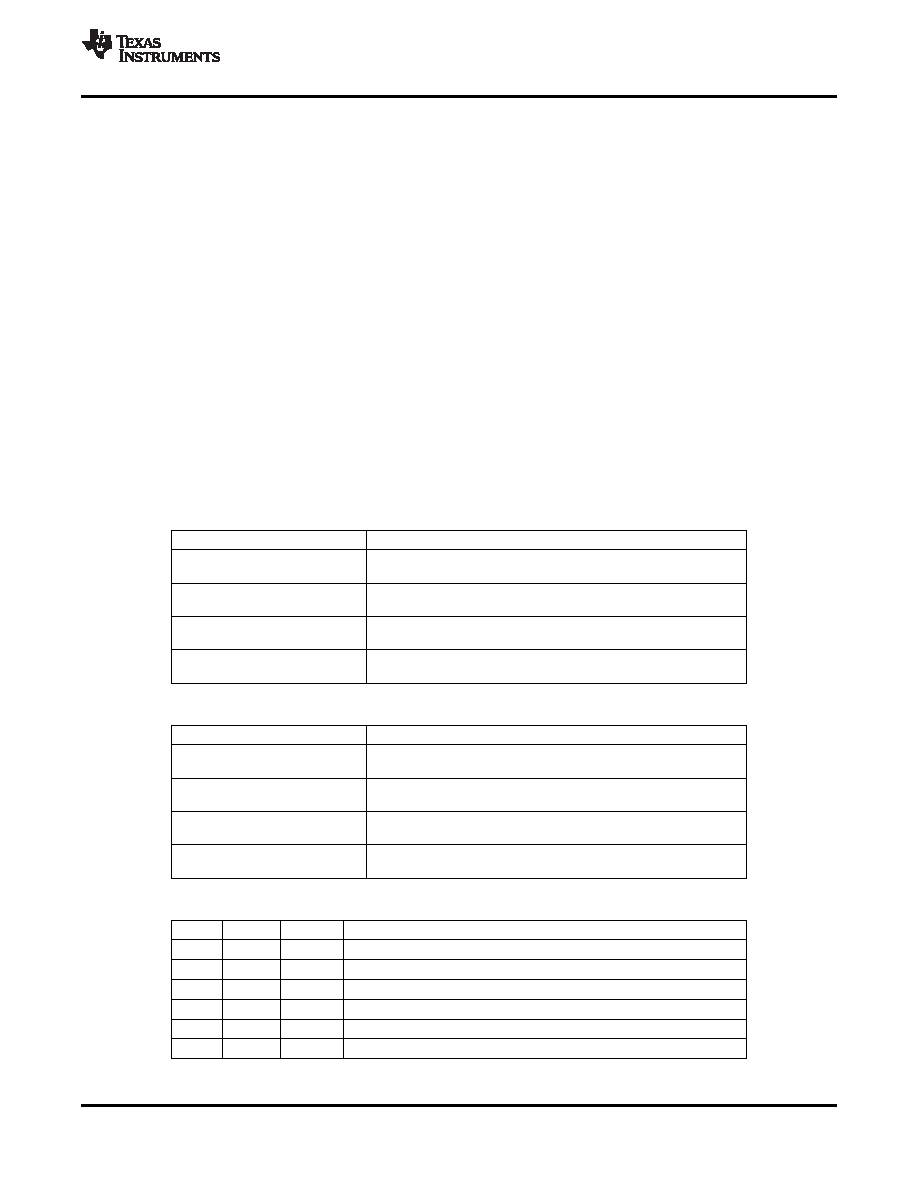
Table 5. SCLK Control Pin
SCLK
DESCRIPTION
0
Internal reference
+200mV/-0mV
(3/8)AVDD
External reference
±200mV
(5/8)2AVDD
External reference
±200mV
AVDD
Internal reference
+0mV/-200mV
Table 6. SEN Control Pin
SEN
DESCRIPTION
0
Offset binary and DDR LVDS output
+200mV/-0mV
(3/8)AVDD
2’s complement format and DDR LVDS output
±200mV
(5/8)2AVDD
2’s complement format and parallel CMOS output
±200mV
AVDD
Offset binary and parallel CMOS output
+0mV/-200mV
Table 7. CTRL1, CTRL2 and CTRL3 Pins
CTRL1
CTRL2
CTRL3
DESCRIPTION
LOW
Normal operation
LOW
HIGH
SNRBoost enabled for Channel B(1)
LOW
HIGH
LOW
SNRBoost enabled for Channel A(1)
LOW
HIGH
SNRBoost enabled for Channel A and B(1)
HIGH
LOW
Global power down
HIGH
LOW
HIGH
Channel B standby
(1)
To enable & disable SNRBoost mode using the CTRL pins, reset the register bits <SNRBoost Enable -
CHA> = 0 & <SNRBoost Enable - CHB> = 0.
Copyright 2009, Texas Instruments Incorporated
13
Product Folder Link(s): ADS62C17
相关PDF资料 |
PDF描述 |
|---|---|
| D38999/20WG39BN | CONN HSG RCPT 39POS WALL MT SCKT |
| MS3106R22-23P | CONN PLUG 8POS STRAIGHT W/PINS |
| ISL54003IRTZ-T | IC AMP AUDIO PWR 1.23W AB 20TQFN |
| MS3101E24-9P | CONN RCPT 2POS FREE HNG W/PINS |
| CB3100R-18-11S | CONN RCPT 5POS WALL MNT W/SCKT |
相关代理商/技术参数 |
参数描述 |
|---|---|
| ADS62C17IRGCT | 功能描述:模数转换器 - ADC Dual Channel 11B 200MSPS ADC RoHS:否 制造商:Texas Instruments 通道数量:2 结构:Sigma-Delta 转换速率:125 SPs to 8 KSPs 分辨率:24 bit 输入类型:Differential 信噪比:107 dB 接口类型:SPI 工作电源电压:1.7 V to 3.6 V, 2.7 V to 5.25 V 最大工作温度:+ 85 C 安装风格:SMD/SMT 封装 / 箱体:VQFN-32 |
| ADS62P15 | 制造商:TI 制造商全称:Texas Instruments 功能描述:Dual Channel 11-Bits, 125 MSPS ADC With Parallel CMOS/DDR LVDS Outputs |
| ADS62P15_09 | 制造商:TI 制造商全称:Texas Instruments 功能描述:Dual Channel 11-Bits,125 MSPS ADC With Parallel CMOS/DDR LVDS Outputs |
| ADS62P15_1 | 制造商:TI 制造商全称:Texas Instruments 功能描述:Dual Channel 11-Bits,125 MSPS ADC With Parallel CMOS/DDR LVDS Outputs |
| ADS62P15EVM | 功能描述:数据转换 IC 开发工具 ADS62P15 Eval Mod RoHS:否 制造商:Texas Instruments 产品:Demonstration Kits 类型:ADC 工具用于评估:ADS130E08 接口类型:SPI 工作电源电压:- 6 V to + 6 V |
发布紧急采购,3分钟左右您将得到回复。