- 您现在的位置:买卖IC网 > PDF目录19380 > ADSP-21366BSWZ-1AA (Analog Devices Inc)IC DSP 32BIT 333MHZ EPAD 144LQFP PDF资料下载
参数资料
| 型号: | ADSP-21366BSWZ-1AA |
| 厂商: | Analog Devices Inc |
| 文件页数: | 19/60页 |
| 文件大小: | 0K |
| 描述: | IC DSP 32BIT 333MHZ EPAD 144LQFP |
| 产品培训模块: | SHARC Processor Overview |
| 标准包装: | 1 |
| 系列: | SHARC® |
| 类型: | 浮点 |
| 接口: | DAI,SPI |
| 时钟速率: | 333MHz |
| 非易失内存: | ROM(512 kB) |
| 芯片上RAM: | 384kB |
| 电压 - 输入/输出: | 3.30V |
| 电压 - 核心: | 1.20V |
| 工作温度: | -40°C ~ 85°C |
| 安装类型: | 表面贴装 |
| 封装/外壳: | 144-LQFP 裸露焊盘 |
| 供应商设备封装: | 144-LQFP(20x20) |
| 包装: | 托盘 |
第1页第2页第3页第4页第5页第6页第7页第8页第9页第10页第11页第12页第13页第14页第15页第16页第17页第18页当前第19页第20页第21页第22页第23页第24页第25页第26页第27页第28页第29页第30页第31页第32页第33页第34页第35页第36页第37页第38页第39页第40页第41页第42页第43页第44页第45页第46页第47页第48页第49页第50页第51页第52页第53页第54页第55页第56页第57页第58页第59页第60页
�� �
�
�ADSP-21362/ADSP-21363/ADSP-21364/ADSP-21365/ADSP-21366�
�Clock� Input�
�Table� 11.� Clock� Input�
�200� MHz� 1�
�333� MHz� 2�
�Parameter�
�Min�
�Max�
�Min�
�Max�
�Unit�
�Timing� Requirements�
�t� CK�
�CLKIN� Period�
�30� 3�
�100�
�18�
�100�
�ns�
�t� CKL�
�t� CKH�
�t� CKRF�
�CLKIN� Width� Low�
�CLKIN� Width� High�
�CLKIN� Rise/Fall� (0.4� V� to� 2.0� V)�
�12.5�
�12.5�
�3�
�7.5�
�7.5�
�3�
�ns�
�ns�
�ns�
�t� CCLK� 4�
�t� VCO� 5�
�t� CKJ� 6,� 7�
�CCLK� Period�
�VCO� Frequency�
�CLKIN� Jitter� Tolerance�
�5.0�
�200�
�–250�
�10�
�600�
�+250�
�3.0�
�200�
�–250�
�10�
�800�
�+250�
�ns�
�MHz�
�ps�
�1�
�2�
�3�
�4�
�5�
�6�
�7�
���Applies� only� for� CLK_CFG1–0� =� 00� and� default� values� for� PLL� control� bits� in� the� PMCTL� register.�
�Any� changes� to� PLL� control� bits� in� the� PMCTL� register� must� meet� core� clock� timing� specification� t� CCLK� .�
�See� Figure� 5� on� Page� 17� for� VCO� diagram.�
�Actual� input� jitter� should� be� combined� with� AC� specifications� for� accurate� timing� analysis.�
�Jitter� specification� is� maximum� peak-to-peak� time� interval� error� (TIE)� jitter.�
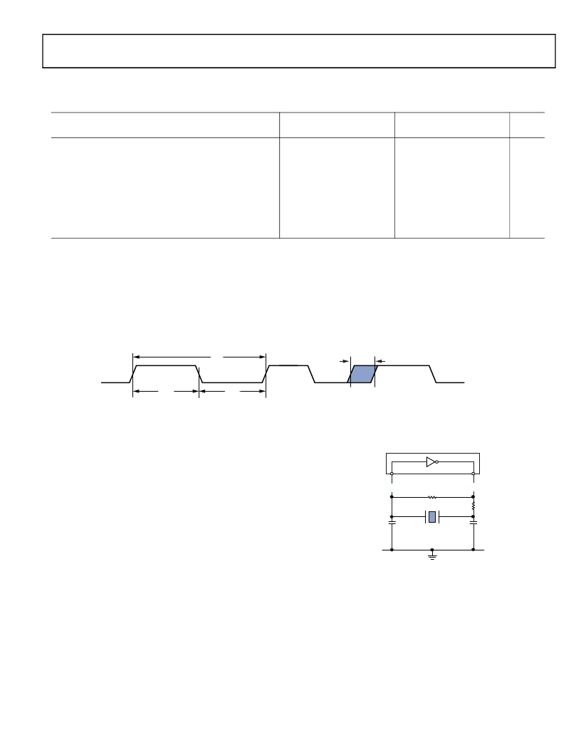
�CLKIN�
�t� CKH�
�t� CK�
�t� CKL�
�t� CKJ�
�Figure� 7.� Clock� Input�
�Clock� Signals�
�The� processor� can� use� an� external� clock� or� a� crystal.� Refer� to� the�
�CLKIN� pin� description� in� Table� 6� on� Page� 11� .� The� user� applica-�
�ADSP-2136x�
�tion� program� can� configure� the� processor� to� use� its� internal�
�clock� generator� by� connecting� the� necessary� components� to� the�
�CLKIN� and� XTAL� pins.� Figure� 8� shows� the� component� connec-�
�tions� used� for� a� fundamental� frequency� crystal� operating� in�
�parallel� mode.�
�Note� that� the� clock� rate� is� achieved� using� a� 16.67� MHz� crystal�
�CLKIN�
�C1�
�22pF�
�R1�
�1M� Ω� *�
�Y1�
�24.576MHz�
�XTAL�
�R2�
�47� Ω� *�
�C2�
�22pF�
�and� a� PLL� multiplier� ratio� 16:1.� (CCLK:CLKIN� achieves� a� clock�
�speed� of� 266.72� MHz.)� To� achieve� the� full� core� clock� rate,� pro-�
�grams� need� to� configure� the� multiplier� bits� in� the�
�PMCTL� register.�
�R2� SHOULD� BE� CHOSEN� TO� LIMIT� CRYSTAL�
�DRIVE� POWER.� REFER� TO� CRYSTAL�
�MANUFACTURER’S� SPECIFICATIONS.�
�*TYPICAL� VALUES�
�Figure� 8.� Recommended� Circuit� for� Fundamental� Mode� Crystal� Operation�
�Rev.� J� |�
�Page� 19� of� 60� |�
�July� 2013�
�相关PDF资料 |
PDF描述 |
|---|---|
| RSM40DRMH-S288 | CONN EDGECARD 80POS .156 EXTEND |
| VE-21T-CW-F2 | CONVERTER MOD DC/DC 6.5V 100W |
| RS3-0512S/H2 | CONV DC/DC 3W 4.5-9VIN 12VOUT |
| EBC12DCSD | CONN EDGECARD 24POS DIP .100 SLD |
| RMM40DRMH-S288 | CONN EDGECARD 80POS .156 EXTEND |
相关代理商/技术参数 |
参数描述 |
|---|---|
| ADSP-21366KBC-1AA | 功能描述:数字信号处理器和控制器 - DSP, DSC 333 MHz SHARC with on chipRom RoHS:否 制造商:Microchip Technology 核心:dsPIC 数据总线宽度:16 bit 程序存储器大小:16 KB 数据 RAM 大小:2 KB 最大时钟频率:40 MHz 可编程输入/输出端数量:35 定时器数量:3 设备每秒兆指令数:50 MIPs 工作电源电压:3.3 V 最大工作温度:+ 85 C 封装 / 箱体:TQFP-44 安装风格:SMD/SMT |
| ADSP-21366KBCZ1AA | 制造商:Analog Devices 功能描述:- Trays |
| ADSP-21366KBCZ-1AA | 功能描述:数字信号处理器和控制器 - DSP, DSC es3 MHz SHARC with on chipRom RoHS:否 制造商:Microchip Technology 核心:dsPIC 数据总线宽度:16 bit 程序存储器大小:16 KB 数据 RAM 大小:2 KB 最大时钟频率:40 MHz 可编程输入/输出端数量:35 定时器数量:3 设备每秒兆指令数:50 MIPs 工作电源电压:3.3 V 最大工作温度:+ 85 C 封装 / 箱体:TQFP-44 安装风格:SMD/SMT |
| ADSP-21366KSWZ-1AA | 制造商:Analog Devices 功能描述:DSP FLOATING PT 32BIT/40-BIT 333MHZ 333MIPS 144LQFP EP - Trays 制造商:Analog Devices 功能描述:IC SHARC DSP 333MHZ SMD LQFP144 |
| ADSP-21366SBBC-ENG | 制造商:AD 制造商全称:Analog Devices 功能描述:SHARC Processor |
发布紧急采购,3分钟左右您将得到回复。