- 您现在的位置:买卖IC网 > PDF目录19389 > ADSP-BF544MBBCZ-5M (Analog Devices Inc)IC DSP 16BIT 533MHZ MDDR 400CBGA PDF资料下载
参数资料
| 型号: | ADSP-BF544MBBCZ-5M |
| 厂商: | Analog Devices Inc |
| 文件页数: | 11/100页 |
| 文件大小: | 0K |
| 描述: | IC DSP 16BIT 533MHZ MDDR 400CBGA |
| 标准包装: | 1 |
| 系列: | Blackfin® |
| 类型: | 定点 |
| 接口: | CAN,SPI,SSP,TWI,UART |
| 时钟速率: | 533MHz |
| 非易失内存: | 外部 |
| 芯片上RAM: | 196kB |
| 电压 - 输入/输出: | 2.50V,3.30V |
| 电压 - 核心: | 1.25V |
| 工作温度: | -40°C ~ 85°C |
| 安装类型: | 表面贴装 |
| 封装/外壳: | 400-LFBGA,CSPBGA |
| 供应商设备封装: | 400-CSPBGA(17x17) |
| 包装: | 托盘 |
| 配用: | ADZS-BF548-EZLITE-ND - KIT EZLITE ADZS-BF548 |
第1页第2页第3页第4页第5页第6页第7页第8页第9页第10页当前第11页第12页第13页第14页第15页第16页第17页第18页第19页第20页第21页第22页第23页第24页第25页第26页第27页第28页第29页第30页第31页第32页第33页第34页第35页第36页第37页第38页第39页第40页第41页第42页第43页第44页第45页第46页第47页第48页第49页第50页第51页第52页第53页第54页第55页第56页第57页第58页第59页第60页第61页第62页第63页第64页第65页第66页第67页第68页第69页第70页第71页第72页第73页第74页第75页第76页第77页第78页第79页第80页第81页第82页第83页第84页第85页第86页第87页第88页第89页第90页第91页第92页第93页第94页第95页第96页第97页第98页第99页第100页
Rev. C
|
Page 18 of 100
|
February 2010
ADSP-BF542/ADSP-BF544/ADSP-BF547/ADSP-BF548/ADSP-BF549
Power Domains
As shown in Table 6, the ADSP-BF54x Blackfin processors sup-
port different power domains. The use of multiple power
domains maximizes flexibility while maintaining compliance
with industry standards and conventions. By isolating the inter-
nal logic of the ADSP-BF54x Blackfin processors into its own
power domain separate from the RTC and other I/O, the pro-
cessors can take advantage of dynamic power management
without affecting the RTC or other I/O devices. There are no
sequencing requirements for the various power domains.
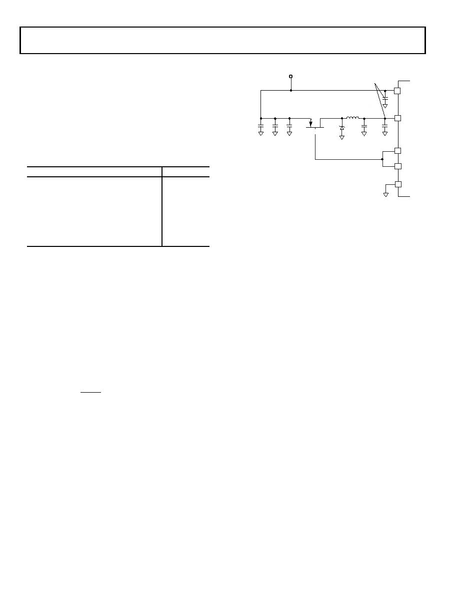
VOLTAGE REGULATION
The ADSP-BF54x Blackfin processors provide an on-chip volt-
age regulator that can generate processor core voltage levels
from an external supply (see specifications in Operating Condi-
tions on Page 34). Figure 6 on Page 18 shows the typical
external components required to complete the power manage-
ment system. The regulator controls the internal logic voltage
levels and is programmable with the voltage regulator control
register (VR_CTL) in increments of 50 mV. This register can be
accessed using the bfrom_SysControl() function in the on-chip
ROM. To reduce standby power consumption, the internal volt-
age regulator can be programmed to remove power to the
processor core while keeping I/O power supplied. While in
hibernate state, VDDEXT, VDDRTC, VDDDDR, VDDUSB, and VDDVR can
still be applied, eliminating the need for external buffers. The
voltage regulator can be activated from this power-down state
by assertion of the RESET pin, which then initiates a boot
sequence. The regulator can also be disabled and bypassed at the
user’s discretion. For all 600 MHz speed grade models and all
automotive grade models, the internal voltage regulator must
not be used and VDDVR must be tied to VDDEXT. For additional
information regarding design of the voltage regulator circuit,
see Switching Regulator Design Considerations for the ADSP-
BF533 Blackfin Processors (EE-228).
CLOCK SIGNALS
The ADSP-BF54x Blackfin processors can be clocked by an
external crystal, a sine wave input, or a buffered, shaped clock
derived from an external clock oscillator.
If an external clock is used, it should be a TTL-compatible signal
and must not be halted, changed, or operated below the speci-
fied frequency during normal operation. This signal is
connected to the processor’s CLKIN pin. When an external
clock is used, the XTAL pin must be left unconnected.
Alternatively, because the ADSP-BF54x Blackfin processors
include an on-chip oscillator circuit, an external crystal may be
used. For fundamental frequency operation, use the circuit
shown in Figure 7. A parallel-resonant, fundamental frequency,
microprocessor-grade crystal is connected across the CLKIN
and XTAL pins. The on-chip resistance between CLKIN and the
XTAL pin is in the 500 k
range. Typically, further parallel
resistors are not recommended. The two capacitors and the
series resistor shown in Figure 7 fine-tune phase and amplitude
of the sine frequency. The 1MOhm pull-up resistor on the
XTAL pin guarantees that the clock circuit is properly held inac-
tive when the processor is in the hibernate state.
The capacitor and resistor values shown in Figure 7 are typical
values only. The capacitor values are dependent upon the crystal
manufacturers’ load capacitance recommendations and the PCB
physical layout. The resistor value depends on the drive level
specified by the crystal manufacturer. System designs should
verify the customized values based on careful investigations on
multiple devices over temperature range.
Table 6. Power Domains
Power Domain
VDD Range
All internal logic, except RTC, DDR, and USB
VDDINT
RTC internal logic and crystal I/O
VDDRTC
DDR external memory supply
VDDDDR
USB internal logic and crystal I/O
VDDUSB
Internal voltage regulator
VDDVR
MXVR PLL and logic
VDDMP
All other I/O
VDDEXT
Figure 6. Voltage Regulator Circuit
VDDVR
(LOW-INDUCTANCE)
VDDINT
VROUT
100μF
VROUT
GND
SHORT AND LOW-
INDUCTANCE WIRE
VDDVR
+
100μF
10μF
LOW ESR
100nF
SETOFDECOUPLING
CAPACITORS
FDS9431A
ZHCS1000
2.7V TO 3.6V
INPUT VOLTAGE
RANGE
NOTE: DESIGNER SHOULD MINIMIZE
TRACE LENGTH TO FDS9431A.
10μH
相关PDF资料 |
PDF描述 |
|---|---|
| SWS600L-5 | POWER SUPPLY 5V 120A SGL OUTPUT |
| ADSP-BF544BBCZ-5A | IC DSP 16BIT 533MHZ 400CSBGA |
| ADSP-21266SKSTZ-2D | IC DSP 32BIT 150MHZ 144-LQFP |
| ADSP-BF534BBC-5A | IC DSP CTLR 16BIT 182CSPBGA |
| MAX6643LBBAEE+T | IC CNTRLR FAN SPEED 16-QSOP |
相关代理商/技术参数 |
参数描述 |
|---|---|
| ADSP-BF547BBCZ-5A | 功能描述:IC DSP 16BIT 533MHZ 400CSBGA RoHS:是 类别:集成电路 (IC) >> 嵌入式 - DSP(数字式信号处理器) 系列:Blackfin® 标准包装:40 系列:TMS320DM64x, DaVinci™ 类型:定点 接口:I²C,McASP,McBSP 时钟速率:400MHz 非易失内存:外部 芯片上RAM:160kB 电压 - 输入/输出:3.30V 电压 - 核心:1.20V 工作温度:0°C ~ 90°C 安装类型:表面贴装 封装/外壳:548-BBGA,FCBGA 供应商设备封装:548-FCBGA(27x27) 包装:托盘 配用:TMDSDMK642-0E-ND - DEVELPER KIT W/NTSC CAMERA296-23038-ND - DSP STARTER KIT FOR TMS320C6416296-23059-ND - FLASHBURN PORTING KIT296-23058-ND - EVAL MODULE FOR DM642TMDSDMK642-ND - DEVELOPER KIT W/NTSC CAMERA |
| ADSP-BF547BBCZ-5X | 制造商:Analog Devices 功能描述:- Trays |
| ADSP-BF547BBCZC11 | 制造商:Analog Devices 功能描述: |
| ADSP-BF547KBCZ-6A | 功能描述:IC DSP 600MHZ 400CSPBGA RoHS:是 类别:集成电路 (IC) >> 嵌入式 - DSP(数字式信号处理器) 系列:Blackfin® 标准包装:40 系列:TMS320DM64x, DaVinci™ 类型:定点 接口:I²C,McASP,McBSP 时钟速率:400MHz 非易失内存:外部 芯片上RAM:160kB 电压 - 输入/输出:3.30V 电压 - 核心:1.20V 工作温度:0°C ~ 90°C 安装类型:表面贴装 封装/外壳:548-BBGA,FCBGA 供应商设备封装:548-FCBGA(27x27) 包装:托盘 配用:TMDSDMK642-0E-ND - DEVELPER KIT W/NTSC CAMERA296-23038-ND - DSP STARTER KIT FOR TMS320C6416296-23059-ND - FLASHBURN PORTING KIT296-23058-ND - EVAL MODULE FOR DM642TMDSDMK642-ND - DEVELOPER KIT W/NTSC CAMERA |
| ADSP-BF547MBBCZ-5M | 功能描述:IC DSP 16BIT 533MHZ MDDR 400CBGA RoHS:是 类别:集成电路 (IC) >> 嵌入式 - DSP(数字式信号处理器) 系列:Blackfin® 标准包装:40 系列:TMS320DM64x, DaVinci™ 类型:定点 接口:I²C,McASP,McBSP 时钟速率:400MHz 非易失内存:外部 芯片上RAM:160kB 电压 - 输入/输出:3.30V 电压 - 核心:1.20V 工作温度:0°C ~ 90°C 安装类型:表面贴装 封装/外壳:548-BBGA,FCBGA 供应商设备封装:548-FCBGA(27x27) 包装:托盘 配用:TMDSDMK642-0E-ND - DEVELPER KIT W/NTSC CAMERA296-23038-ND - DSP STARTER KIT FOR TMS320C6416296-23059-ND - FLASHBURN PORTING KIT296-23058-ND - EVAL MODULE FOR DM642TMDSDMK642-ND - DEVELOPER KIT W/NTSC CAMERA |
发布紧急采购,3分钟左右您将得到回复。