参数资料
| 型号: | ADUC7122BBCZ-RL |
| 厂商: | Analog Devices Inc |
| 文件页数: | 20/96页 |
| 文件大小: | 0K |
| 描述: | PRECISION ANALOG MCU I.C |
| 标准包装: | 1 |
| 系列: | MicroConverter® ADuC7xxx |
| 核心处理器: | ARM7 |
| 芯体尺寸: | 16/32-位 |
| 速度: | 41.78MHz |
| 连通性: | I²C,SPI,UART/USART |
| 外围设备: | POR,PWM,WDT |
| 输入/输出数: | 32 |
| 程序存储器容量: | 126KB(63K x 16) |
| 程序存储器类型: | 闪存 |
| RAM 容量: | 8K x 8 |
| 电压 - 电源 (Vcc/Vdd): | 3 V ~ 3.6 V |
| 数据转换器: | A/D 13x12b,D/A 12x12b |
| 振荡器型: | 内部 |
| 工作温度: | -10°C ~ 95°C |
| 封装/外壳: | 108-LFBGA,CSPBGA |
| 包装: | 标准包装 |
| 其它名称: | ADUC7122BBCZ-RLDKR |
第1页第2页第3页第4页第5页第6页第7页第8页第9页第10页第11页第12页第13页第14页第15页第16页第17页第18页第19页当前第20页第21页第22页第23页第24页第25页第26页第27页第28页第29页第30页第31页第32页第33页第34页第35页第36页第37页第38页第39页第40页第41页第42页第43页第44页第45页第46页第47页第48页第49页第50页第51页第52页第53页第54页第55页第56页第57页第58页第59页第60页第61页第62页第63页第64页第65页第66页第67页第68页第69页第70页第71页第72页第73页第74页第75页第76页第77页第78页第79页第80页第81页第82页第83页第84页第85页第86页第87页第88页第89页第90页第91页第92页第93页第94页第95页第96页
ADuC7122
Rev. 0 | Page 27 of 96
ADC CIRCUIT OVERVIEW
The analog-to-digital converter (ADC) incorporates a fast,
multichannel, 12-bit ADC. It can operate from 3.0 V to 3.6 V
supplies and is capable of providing a throughput of up to 1 MSPS
when the clock source is 41.78 MHz. This block provides the
user with a multichannel multiplexer, differential track-and-
hold, on-chip reference, and ADC.
The ADC consists of a 12-bit successive approximation converter
based around two capacitor DACs. Depending on the input
signal configuration, the ADC can operate in one of the
following three modes:
Fully differential mode for small and balanced signals
Single-ended mode for any single-ended signals
Pseudo differential mode for any single-ended signals,
taking advantage of the common-mode rejection offered
by the pseudo differential input
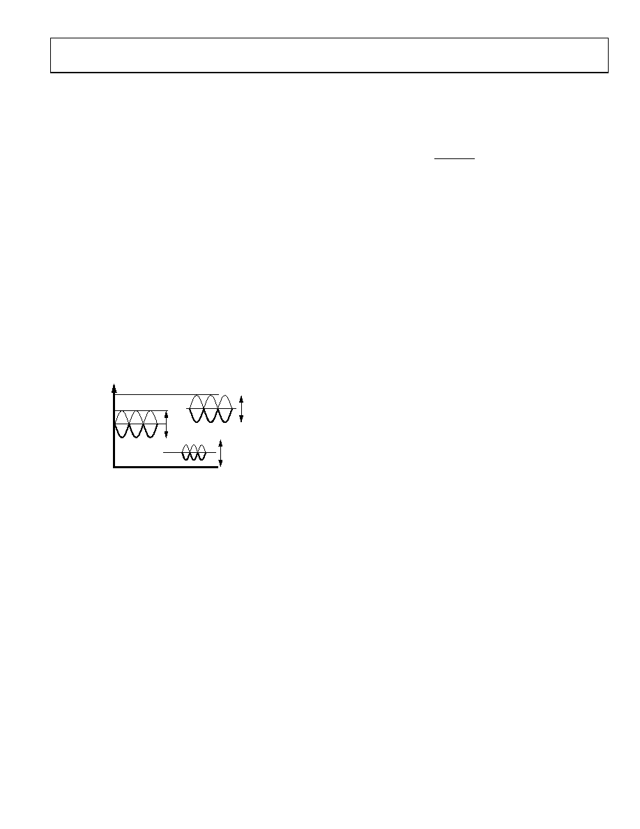
The converter accepts an analog input range of 0 to VREF when
operating in single-ended mode or pseudo differential mode. In
fully differential mode, the input signal must be balanced around
a common-mode voltage, VCM, in the range 0 V to AVDD, and
AVDD
VCM
0
2VREF
0
87
55
-01
2
Figure 12. Examples of Balanced Signals for Fully Differential Mode
A high precision, low drift, and factory-calibrated 2.5 V reference
is provided on chip. An external reference can also be connected
as described in the Band Gap Reference section.
Single or continuous conversion modes can be initiated in
software. An external CONVST pin, an output generated from
the on-chip PLA, or a Timer0 or Timer1 overflow can also be
used to generate a repetitive trigger for ADC conversions.
If the signal has not been deasserted by the time the ADC
conversion is complete, a second conversion begins
automatically.
A voltage output from an on-chip band gap reference propor-
tional to absolute temperature can also be routed through the
front-end ADC multiplexer, effectively an additional ADC
channel input. This facilitates an internal temperature sensor
channel, measuring die temperature to an accuracy of 3C.
For the ADuC7122, a number of modifications have been made
to the ADC input structure that appears in the ADuC702x
family.
The PADC0 and PADC1 inputs connect to a PGA in pseudo
differential mode and allow for selectable gains from 1 to 5 with
32 steps. The remaining ADC channels can be configured as
single, differential, or pseudo differential. A buffer is provided
before the ADC for measuring internal channels.
相关PDF资料 |
PDF描述 |
|---|---|
| ADUC7126BSTZ126-RL | IC MCU 16/32B 126KB FLASH 80LQFP |
| ADUC7129BSTZ126 | IC DAS MCU ARM7 ADC/DDS 80-LQFP |
| ADUC812BSZ-REEL | IC MCU FLASH 12BIT ADC 52MQFP |
| ADUC814BRU | IC ADC 12BIT W/FLASH MCU 28TSSOP |
| ADUC816BCP | IC MCU 8K FLASH ADC/DAC 56LFCSP |
相关代理商/技术参数 |
参数描述 |
|---|---|
| ADUC7124 | 制造商:AD 制造商全称:Analog Devices 功能描述:Precision Analog Microcontroller, 12-Bit Analog I/O, Large Memory, ARM7TDMI MCU with Enhanced IRQ Handler |
| ADUC7124BCPZ126 | 功能描述:IC DAS MCU ARM7 ADC/DDS 64LQFP RoHS:是 类别:集成电路 (IC) >> 嵌入式 - 微控制器, 系列:MicroConverter® ADuC7xxx 标准包装:250 系列:LPC11Uxx 核心处理器:ARM? Cortex?-M0 芯体尺寸:32-位 速度:50MHz 连通性:I²C,Microwire,SPI,SSI,SSP,UART/USART,USB 外围设备:欠压检测/复位,POR,WDT 输入/输出数:40 程序存储器容量:96KB(96K x 8) 程序存储器类型:闪存 EEPROM 大小:4K x 8 RAM 容量:10K x 8 电压 - 电源 (Vcc/Vdd):1.8 V ~ 3.6 V 数据转换器:A/D 8x10b 振荡器型:内部 工作温度:-40°C ~ 85°C 封装/外壳:48-LQFP 包装:托盘 其它名称:568-9587 |
| ADUC7124BCPZ126-RL | 功能描述:IC DAS MCU ARM7 ADC/DDS 64-LQFP RoHS:是 类别:集成电路 (IC) >> 嵌入式 - 微控制器, 系列:MicroConverter® ADuC7xxx 标准包装:38 系列:Encore!® XP® 核心处理器:eZ8 芯体尺寸:8-位 速度:5MHz 连通性:IrDA,UART/USART 外围设备:欠压检测/复位,LED,POR,PWM,WDT 输入/输出数:16 程序存储器容量:4KB(4K x 8) 程序存储器类型:闪存 EEPROM 大小:- RAM 容量:1K x 8 电压 - 电源 (Vcc/Vdd):2.7 V ~ 3.6 V 数据转换器:- 振荡器型:内部 工作温度:-40°C ~ 105°C 封装/外壳:20-SOIC(0.295",7.50mm 宽) 包装:管件 其它名称:269-4116Z8F0413SH005EG-ND |
| ADUC7126BSTZ126 | 功能描述:IC MCU 16/32B 126KB FLASH 80LQFP RoHS:是 类别:集成电路 (IC) >> 嵌入式 - 微控制器, 系列:MicroConverter® ADuC7xxx 标准包装:250 系列:LPC11Uxx 核心处理器:ARM? Cortex?-M0 芯体尺寸:32-位 速度:50MHz 连通性:I²C,Microwire,SPI,SSI,SSP,UART/USART,USB 外围设备:欠压检测/复位,POR,WDT 输入/输出数:40 程序存储器容量:96KB(96K x 8) 程序存储器类型:闪存 EEPROM 大小:4K x 8 RAM 容量:10K x 8 电压 - 电源 (Vcc/Vdd):1.8 V ~ 3.6 V 数据转换器:A/D 8x10b 振荡器型:内部 工作温度:-40°C ~ 85°C 封装/外壳:48-LQFP 包装:托盘 其它名称:568-9587 |
| ADUC7126BSTZ126I | 功能描述:IC MCU 16/32B 126KB FLASH 80LQFP RoHS:是 类别:集成电路 (IC) >> 嵌入式 - 微控制器, 系列:MicroConverter® ADuC7xxx 标准包装:250 系列:LPC11Uxx 核心处理器:ARM? Cortex?-M0 芯体尺寸:32-位 速度:50MHz 连通性:I²C,Microwire,SPI,SSI,SSP,UART/USART,USB 外围设备:欠压检测/复位,POR,WDT 输入/输出数:40 程序存储器容量:96KB(96K x 8) 程序存储器类型:闪存 EEPROM 大小:4K x 8 RAM 容量:10K x 8 电压 - 电源 (Vcc/Vdd):1.8 V ~ 3.6 V 数据转换器:A/D 8x10b 振荡器型:内部 工作温度:-40°C ~ 85°C 封装/外壳:48-LQFP 包装:托盘 其它名称:568-9587 |
发布紧急采购,3分钟左右您将得到回复。