参数资料
| 型号: | ADUC7122BBCZ-RL |
| 厂商: | Analog Devices Inc |
| 文件页数: | 35/96页 |
| 文件大小: | 0K |
| 描述: | PRECISION ANALOG MCU I.C |
| 标准包装: | 1 |
| 系列: | MicroConverter® ADuC7xxx |
| 核心处理器: | ARM7 |
| 芯体尺寸: | 16/32-位 |
| 速度: | 41.78MHz |
| 连通性: | I²C,SPI,UART/USART |
| 外围设备: | POR,PWM,WDT |
| 输入/输出数: | 32 |
| 程序存储器容量: | 126KB(63K x 16) |
| 程序存储器类型: | 闪存 |
| RAM 容量: | 8K x 8 |
| 电压 - 电源 (Vcc/Vdd): | 3 V ~ 3.6 V |
| 数据转换器: | A/D 13x12b,D/A 12x12b |
| 振荡器型: | 内部 |
| 工作温度: | -10°C ~ 95°C |
| 封装/外壳: | 108-LFBGA,CSPBGA |
| 包装: | 标准包装 |
| 其它名称: | ADUC7122BBCZ-RLDKR |
第1页第2页第3页第4页第5页第6页第7页第8页第9页第10页第11页第12页第13页第14页第15页第16页第17页第18页第19页第20页第21页第22页第23页第24页第25页第26页第27页第28页第29页第30页第31页第32页第33页第34页当前第35页第36页第37页第38页第39页第40页第41页第42页第43页第44页第45页第46页第47页第48页第49页第50页第51页第52页第53页第54页第55页第56页第57页第58页第59页第60页第61页第62页第63页第64页第65页第66页第67页第68页第69页第70页第71页第72页第73页第74页第75页第76页第77页第78页第79页第80页第81页第82页第83页第84页第85页第86页第87页第88页第89页第90页第91页第92页第93页第94页第95页第96页
ADuC7122
Rev. 0 | Page 40 of 96
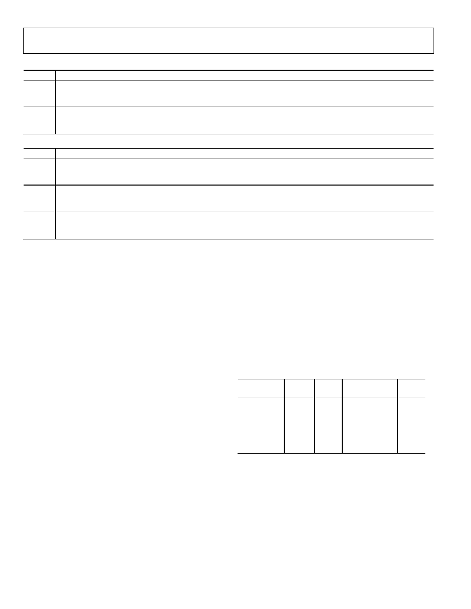
Table 57. FEE0PRO and FEE0HID MMR Bit Designations
Bit
Description
31
Read protection.
Cleared by the user to protect Block 0.
Set by the user to allow reading of Block 0.
30:0
Write protection for Page 123 to Page 120, for Page 119 to Page 116, and for Page 3 to Page 0.
Cleared by the user to protect the pages in writing.
Set by the user to allow writing the pages.
Table 58. FEE1PRO and FEE1HID MMR Bit Designations
Bit
Description
31
Read protection.
Cleared by the user to protect Block 1.
Set by the user to allow reading of Block 1.
30
Write protection for Page 127 to Page 120.
Cleared by the user to protect the pages in writing.
Set by the user to allow writing the pages.
29:0
Write protection for Page 119 to Page 116 and for Page 3 to Page 0.
Cleared by the user to protect the pages in writing.
Set by the user to allow writing the pages.
EXECUTION TIME FROM SRAM AND FLASH/EE
This section describes SRAM and Flash/EE access times during
execution of applications where execution time is critical.
Execution from SRAM
Fetching instructions from SRAM takes one clock cycle because
the access time of the SRAM is 2 ns and a clock cycle is 22 ns
minimum. However, if the instruction involves reading or
writing data to memory, one extra cycle must be added if the
data is in SRAM (or three cycles if the data is in Flash/EE), one
cycle to execute the instruction and two cycles to obtain the
32-bit data from Flash/EE. A control flow instruction, such as a
branch instruction, takes one cycle to fetch, but it also takes
two cycles to fill the pipeline with the new instructions.
Execution from Flash/EE
Because the Flash/EE width is 16 bits and access time for 16-bit
words is 23 ns, execution from Flash/EE cannot be completed in
one cycle (contrary to a SRAM fetch, which can be completed in
a single cycle when CD bits = 0). Dependent on the instruction,
some dead times may be required before accessing data for any
value of CD bits.
In ARM mode, where instructions are 32 bits, two cycles are
needed to fetch any instruction when CD = 0. In Thumb mode,
where instructions are 16 bits, one cycle is needed to fetch any
instruction.
Timing is identical in both modes when executing instructions
that involve using Flash/EE for data memory. If the instruction
to be executed is a control flow instruction, an extra cycle is
needed to decode the new address of the program counter and
then four cycles are needed to fill the pipeline. A data processing
instruction involving only core registers does not require any
extra clock cycles, but if it involves data in Flash/EE, an extra
clock cycle is needed to decode the address of the data and two
cycles to obtain the 32-bit data from Flash/EE. An extra cycle
must also be added before fetching another instruction. Data
transfer instructions are more complex and are summarized in
Table 59. Execution Cycles in ARM/Thumb Mode
Instructions
Fetch
Cycles
Dead
Time
Data Access
Dead
Time
LD
2/1
1
2
1
LDH
2/1
1
LDM/PUSH
2/1
N
2 × N
N
STR
2/1
1
2 × 20 μs
1
STRH
2/1
1
20 μs
1
STRM/POP
2/1
N
2 × N × 20 μs
N
With 1 < N ≤ 16, N is the number of bytes of data to load or
store in the multiple load/store instruction. The SWAP instruction
combines an LD and STR instruction with only one fetch,
giving a total of eight cycles plus 40 μs.
相关PDF资料 |
PDF描述 |
|---|---|
| ADUC7126BSTZ126-RL | IC MCU 16/32B 126KB FLASH 80LQFP |
| ADUC7129BSTZ126 | IC DAS MCU ARM7 ADC/DDS 80-LQFP |
| ADUC812BSZ-REEL | IC MCU FLASH 12BIT ADC 52MQFP |
| ADUC814BRU | IC ADC 12BIT W/FLASH MCU 28TSSOP |
| ADUC816BCP | IC MCU 8K FLASH ADC/DAC 56LFCSP |
相关代理商/技术参数 |
参数描述 |
|---|---|
| ADUC7124 | 制造商:AD 制造商全称:Analog Devices 功能描述:Precision Analog Microcontroller, 12-Bit Analog I/O, Large Memory, ARM7TDMI MCU with Enhanced IRQ Handler |
| ADUC7124BCPZ126 | 功能描述:IC DAS MCU ARM7 ADC/DDS 64LQFP RoHS:是 类别:集成电路 (IC) >> 嵌入式 - 微控制器, 系列:MicroConverter® ADuC7xxx 标准包装:250 系列:LPC11Uxx 核心处理器:ARM? Cortex?-M0 芯体尺寸:32-位 速度:50MHz 连通性:I²C,Microwire,SPI,SSI,SSP,UART/USART,USB 外围设备:欠压检测/复位,POR,WDT 输入/输出数:40 程序存储器容量:96KB(96K x 8) 程序存储器类型:闪存 EEPROM 大小:4K x 8 RAM 容量:10K x 8 电压 - 电源 (Vcc/Vdd):1.8 V ~ 3.6 V 数据转换器:A/D 8x10b 振荡器型:内部 工作温度:-40°C ~ 85°C 封装/外壳:48-LQFP 包装:托盘 其它名称:568-9587 |
| ADUC7124BCPZ126-RL | 功能描述:IC DAS MCU ARM7 ADC/DDS 64-LQFP RoHS:是 类别:集成电路 (IC) >> 嵌入式 - 微控制器, 系列:MicroConverter® ADuC7xxx 标准包装:38 系列:Encore!® XP® 核心处理器:eZ8 芯体尺寸:8-位 速度:5MHz 连通性:IrDA,UART/USART 外围设备:欠压检测/复位,LED,POR,PWM,WDT 输入/输出数:16 程序存储器容量:4KB(4K x 8) 程序存储器类型:闪存 EEPROM 大小:- RAM 容量:1K x 8 电压 - 电源 (Vcc/Vdd):2.7 V ~ 3.6 V 数据转换器:- 振荡器型:内部 工作温度:-40°C ~ 105°C 封装/外壳:20-SOIC(0.295",7.50mm 宽) 包装:管件 其它名称:269-4116Z8F0413SH005EG-ND |
| ADUC7126BSTZ126 | 功能描述:IC MCU 16/32B 126KB FLASH 80LQFP RoHS:是 类别:集成电路 (IC) >> 嵌入式 - 微控制器, 系列:MicroConverter® ADuC7xxx 标准包装:250 系列:LPC11Uxx 核心处理器:ARM? Cortex?-M0 芯体尺寸:32-位 速度:50MHz 连通性:I²C,Microwire,SPI,SSI,SSP,UART/USART,USB 外围设备:欠压检测/复位,POR,WDT 输入/输出数:40 程序存储器容量:96KB(96K x 8) 程序存储器类型:闪存 EEPROM 大小:4K x 8 RAM 容量:10K x 8 电压 - 电源 (Vcc/Vdd):1.8 V ~ 3.6 V 数据转换器:A/D 8x10b 振荡器型:内部 工作温度:-40°C ~ 85°C 封装/外壳:48-LQFP 包装:托盘 其它名称:568-9587 |
| ADUC7126BSTZ126I | 功能描述:IC MCU 16/32B 126KB FLASH 80LQFP RoHS:是 类别:集成电路 (IC) >> 嵌入式 - 微控制器, 系列:MicroConverter® ADuC7xxx 标准包装:250 系列:LPC11Uxx 核心处理器:ARM? Cortex?-M0 芯体尺寸:32-位 速度:50MHz 连通性:I²C,Microwire,SPI,SSI,SSP,UART/USART,USB 外围设备:欠压检测/复位,POR,WDT 输入/输出数:40 程序存储器容量:96KB(96K x 8) 程序存储器类型:闪存 EEPROM 大小:4K x 8 RAM 容量:10K x 8 电压 - 电源 (Vcc/Vdd):1.8 V ~ 3.6 V 数据转换器:A/D 8x10b 振荡器型:内部 工作温度:-40°C ~ 85°C 封装/外壳:48-LQFP 包装:托盘 其它名称:568-9587 |
发布紧急采购,3分钟左右您将得到回复。