参数资料
| 型号: | ADUC7122BBCZ-RL |
| 厂商: | Analog Devices Inc |
| 文件页数: | 49/96页 |
| 文件大小: | 0K |
| 描述: | PRECISION ANALOG MCU I.C |
| 标准包装: | 1 |
| 系列: | MicroConverter® ADuC7xxx |
| 核心处理器: | ARM7 |
| 芯体尺寸: | 16/32-位 |
| 速度: | 41.78MHz |
| 连通性: | I²C,SPI,UART/USART |
| 外围设备: | POR,PWM,WDT |
| 输入/输出数: | 32 |
| 程序存储器容量: | 126KB(63K x 16) |
| 程序存储器类型: | 闪存 |
| RAM 容量: | 8K x 8 |
| 电压 - 电源 (Vcc/Vdd): | 3 V ~ 3.6 V |
| 数据转换器: | A/D 13x12b,D/A 12x12b |
| 振荡器型: | 内部 |
| 工作温度: | -10°C ~ 95°C |
| 封装/外壳: | 108-LFBGA,CSPBGA |
| 包装: | 标准包装 |
| 其它名称: | ADUC7122BBCZ-RLDKR |
第1页第2页第3页第4页第5页第6页第7页第8页第9页第10页第11页第12页第13页第14页第15页第16页第17页第18页第19页第20页第21页第22页第23页第24页第25页第26页第27页第28页第29页第30页第31页第32页第33页第34页第35页第36页第37页第38页第39页第40页第41页第42页第43页第44页第45页第46页第47页第48页当前第49页第50页第51页第52页第53页第54页第55页第56页第57页第58页第59页第60页第61页第62页第63页第64页第65页第66页第67页第68页第69页第70页第71页第72页第73页第74页第75页第76页第77页第78页第79页第80页第81页第82页第83页第84页第85页第86页第87页第88页第89页第90页第91页第92页第93页第94页第95页第96页
ADuC7122
Rev. 0 | Page 53 of 96
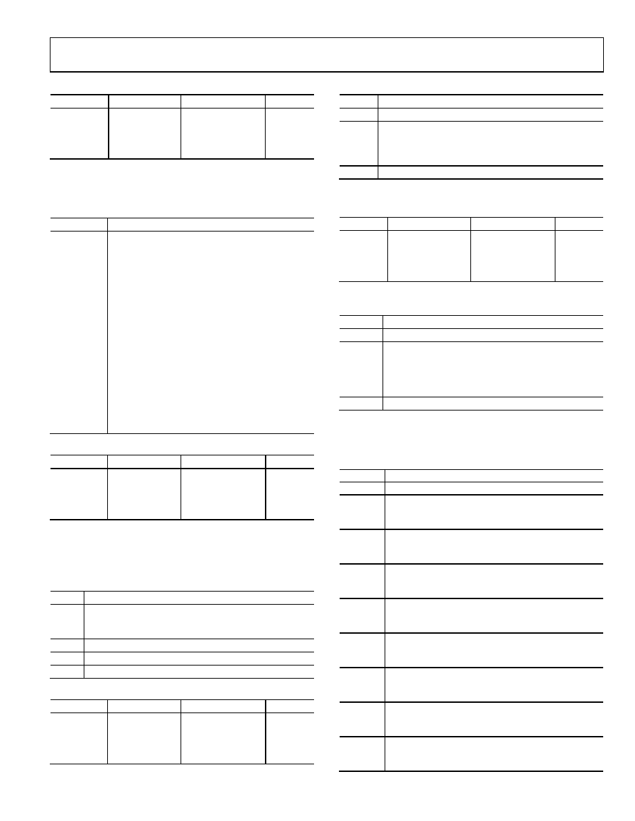
Table 85. GPxPAR Register
Name
Address
Default Value
Access
GP0PAR
0xFFFF0D2C
0x20000000
R/W
GP1PAR
0xFFFF0D3C
0x00000000
R/W
GP2PAR
0xFFFF0D4C
0x00000000
R/W
GP3PAR
0xFFFF0D5C
0x00222222
R/W
GPxPAR programs the parameters for Port 0, Port 1, Port 2, and
Port 3. Note that the GPxDAT MMR must always be written
after changing the GPxPAR MMR.
Table 86. GPxPAR MMR Bit Designations
Bit
Description
31:29
Reserved
28
Pull-up disable Px.7 pin
27:25
Reserved
24
Pull-up disable Px.6 pin
23:21
Reserved
20
Pull-up disable Px.5 pin
19:17
Reserved
16
Pull-up disable Px.4 pin
15:13
Reserved
12
Pull-up disable Px.3 pin
11:9
Reserved
8
Pull-up disable Px.2 pin
7:5
Reserved
4
Pull-up disable Px.1 pin
3:1
Reserved
0
Pull-up disable Px.0 pin
Table 87. GPxDAT Register
Name
Address
Default Value
Access
GP0DAT
0xFFFF0D20
0x000000XX
R/W
GP1DAT
0xFFFF0D30
0x000000XX
R/W
GP2DAT
0xFFFF0D40
0x000000XX
R/W
GP3DAT
0xFFFF0D50
0x000000XX
R/W
GPxDAT is a Port x configuration and data register. It configures
the direction of the GPIO pins of Port x, sets the output value
for the pins configured as outputs, and receives and stores the
input value of the pins configured as inputs.
Table 88. GPxDAT MMR Bit Designations
Bit
Description
31:24
Direction of the data.
Set to 1 by the user to configure the GPIO pin as an output.
Cleared to 0 by user to configure the GPIO pin as an input.
23:16
Port x data output.
15:8
Reflect the state of Port x pins at reset (read only).
7:0
Port x data input (read only).
Table 89. GPxSET Register
Name
Address
Default Value
Access
GP0SET
0xFFFF0D24
0x000000XX
W
GP1SET
0xFFFF0D34
0x000000XX
W
GP2SET
0xFFFF0D44
0x000000XX
W
GP3SET
0xFFFF0D54
0x000000XX
W
Table 90. GPxSET MMR Bit Designations
Bit
Description
31: 24
Reserved.
23:16
Data Port x set bit.
Set to 1 by the user to set bit on Port x; also sets the
corresponding bit in the GPxDAT MMR.
Cleared to 0 by the user; does not affect the data output.
15: 0
Reserved.
GPxSET is a data set Port x register.
Table 91. GPxCLR Register
Name
Address
Default Value
Access
GP0CLR
0xFFFF0D28
0x000000XX
W
GP1CLR
0xFFFF0D38
0x000000XX
W
GP2CLR
0xFFFF0D48
0x000000XX
W
GP3CLR
0xFFFF0D58
0x000000XX
W
GPxCLR is a data clear Port x register.
Table 92. GPxCLR MMR Bit Designations
Bit
Description
31:24
Reserved.
23:16
Data Port x clear bit.
Set to 1 by the user to clear bit on Port x; also clears
the corresponding bit in the GPxDAT MMR.
Cleared to 0 by the user; does not affect the data
output.
15:0
Reserved.
Open-collector functionality is available on the following GPIO
pins: P1.7, P1.6, P2.x, and P3.x. Open-collector functionality can be
configured using GP1OCE[7:6], GP2OCE[7:0], and GP3OCE[7:0].
Table 93. GPxOCE MMR Bit Designations
Bit
Description
31:8
Reserved.
7
GPIO Px.7 open-collector enable
Set to 1 by the user to enable open-collector
Set to 0 by the user to disable open collector
6
GPIO Px.6 open-collector enable
Set to 1 by the user to enable open-collector
Set to 0 by the user to disable open-collector
5
GPIO Px.5 open-collector enable
Set to 1 by the user to enable open-collector
Set to 0 by the user to disable open-collector
4
GPIO Px.4 open-collector enable
Set to 1 by the user to enable open-collector
Set to 0 by the user to disable open-collector
3
GPIO Px.3 open-collector enable
Set to 1 by the user to enable open-collector
Set to 0 by the user to disable open-collector
2
GPIO Px.2 open-collector enable
Set to 1 by the user to enable open-collector
Set to 0 by the user to disable open-collector
1
GPIO Px.1 open-collector enable
Set to 1 by the user to enable open-collector
Set to 0 by the user to disable open-collector
0
GPIO Px.0 open-collector enable
Set to 1 by the user to enable open-collector
Set to 0 by the user to disable open-collector
相关PDF资料 |
PDF描述 |
|---|---|
| ADUC7126BSTZ126-RL | IC MCU 16/32B 126KB FLASH 80LQFP |
| ADUC7129BSTZ126 | IC DAS MCU ARM7 ADC/DDS 80-LQFP |
| ADUC812BSZ-REEL | IC MCU FLASH 12BIT ADC 52MQFP |
| ADUC814BRU | IC ADC 12BIT W/FLASH MCU 28TSSOP |
| ADUC816BCP | IC MCU 8K FLASH ADC/DAC 56LFCSP |
相关代理商/技术参数 |
参数描述 |
|---|---|
| ADUC7124 | 制造商:AD 制造商全称:Analog Devices 功能描述:Precision Analog Microcontroller, 12-Bit Analog I/O, Large Memory, ARM7TDMI MCU with Enhanced IRQ Handler |
| ADUC7124BCPZ126 | 功能描述:IC DAS MCU ARM7 ADC/DDS 64LQFP RoHS:是 类别:集成电路 (IC) >> 嵌入式 - 微控制器, 系列:MicroConverter® ADuC7xxx 标准包装:250 系列:LPC11Uxx 核心处理器:ARM? Cortex?-M0 芯体尺寸:32-位 速度:50MHz 连通性:I²C,Microwire,SPI,SSI,SSP,UART/USART,USB 外围设备:欠压检测/复位,POR,WDT 输入/输出数:40 程序存储器容量:96KB(96K x 8) 程序存储器类型:闪存 EEPROM 大小:4K x 8 RAM 容量:10K x 8 电压 - 电源 (Vcc/Vdd):1.8 V ~ 3.6 V 数据转换器:A/D 8x10b 振荡器型:内部 工作温度:-40°C ~ 85°C 封装/外壳:48-LQFP 包装:托盘 其它名称:568-9587 |
| ADUC7124BCPZ126-RL | 功能描述:IC DAS MCU ARM7 ADC/DDS 64-LQFP RoHS:是 类别:集成电路 (IC) >> 嵌入式 - 微控制器, 系列:MicroConverter® ADuC7xxx 标准包装:38 系列:Encore!® XP® 核心处理器:eZ8 芯体尺寸:8-位 速度:5MHz 连通性:IrDA,UART/USART 外围设备:欠压检测/复位,LED,POR,PWM,WDT 输入/输出数:16 程序存储器容量:4KB(4K x 8) 程序存储器类型:闪存 EEPROM 大小:- RAM 容量:1K x 8 电压 - 电源 (Vcc/Vdd):2.7 V ~ 3.6 V 数据转换器:- 振荡器型:内部 工作温度:-40°C ~ 105°C 封装/外壳:20-SOIC(0.295",7.50mm 宽) 包装:管件 其它名称:269-4116Z8F0413SH005EG-ND |
| ADUC7126BSTZ126 | 功能描述:IC MCU 16/32B 126KB FLASH 80LQFP RoHS:是 类别:集成电路 (IC) >> 嵌入式 - 微控制器, 系列:MicroConverter® ADuC7xxx 标准包装:250 系列:LPC11Uxx 核心处理器:ARM? Cortex?-M0 芯体尺寸:32-位 速度:50MHz 连通性:I²C,Microwire,SPI,SSI,SSP,UART/USART,USB 外围设备:欠压检测/复位,POR,WDT 输入/输出数:40 程序存储器容量:96KB(96K x 8) 程序存储器类型:闪存 EEPROM 大小:4K x 8 RAM 容量:10K x 8 电压 - 电源 (Vcc/Vdd):1.8 V ~ 3.6 V 数据转换器:A/D 8x10b 振荡器型:内部 工作温度:-40°C ~ 85°C 封装/外壳:48-LQFP 包装:托盘 其它名称:568-9587 |
| ADUC7126BSTZ126I | 功能描述:IC MCU 16/32B 126KB FLASH 80LQFP RoHS:是 类别:集成电路 (IC) >> 嵌入式 - 微控制器, 系列:MicroConverter® ADuC7xxx 标准包装:250 系列:LPC11Uxx 核心处理器:ARM? Cortex?-M0 芯体尺寸:32-位 速度:50MHz 连通性:I²C,Microwire,SPI,SSI,SSP,UART/USART,USB 外围设备:欠压检测/复位,POR,WDT 输入/输出数:40 程序存储器容量:96KB(96K x 8) 程序存储器类型:闪存 EEPROM 大小:4K x 8 RAM 容量:10K x 8 电压 - 电源 (Vcc/Vdd):1.8 V ~ 3.6 V 数据转换器:A/D 8x10b 振荡器型:内部 工作温度:-40°C ~ 85°C 封装/外壳:48-LQFP 包装:托盘 其它名称:568-9587 |
发布紧急采购,3分钟左右您将得到回复。