参数资料
| 型号: | ADUC836BCPZ |
| 厂商: | Analog Devices Inc |
| 文件页数: | 26/80页 |
| 文件大小: | 0K |
| 描述: | IC MCU 62K FLASH ADC/DAC 56LFCSP |
| 标准包装: | 1 |
| 系列: | MicroConverter® ADuC8xx |
| 核心处理器: | 8052 |
| 芯体尺寸: | 8-位 |
| 速度: | 12.58MHz |
| 连通性: | EBI/EMI,I²C,SPI,UART/USART |
| 外围设备: | POR,PSM,PWM,温度传感器,WDT |
| 输入/输出数: | 34 |
| 程序存储器容量: | 62KB(62K x 8) |
| 程序存储器类型: | 闪存 |
| EEPROM 大小: | 4K x 8 |
| RAM 容量: | 2.25K x 8 |
| 电压 - 电源 (Vcc/Vdd): | 2.7 V ~ 5.25 V |
| 数据转换器: | A/D 7x16b; D/A 1x12b |
| 振荡器型: | 内部 |
| 工作温度: | -40°C ~ 85°C |
| 封装/外壳: | 56-VFQFN 裸露焊盘,CSP |
| 包装: | 托盘 |
第1页第2页第3页第4页第5页第6页第7页第8页第9页第10页第11页第12页第13页第14页第15页第16页第17页第18页第19页第20页第21页第22页第23页第24页第25页当前第26页第27页第28页第29页第30页第31页第32页第33页第34页第35页第36页第37页第38页第39页第40页第41页第42页第43页第44页第45页第46页第47页第48页第49页第50页第51页第52页第53页第54页第55页第56页第57页第58页第59页第60页第61页第62页第63页第64页第65页第66页第67页第68页第69页第70页第71页第72页第73页第74页第75页第76页第77页第78页第79页第80页
ADuC836
–32–
ADuC836
–33–
Using the Flash/EE Data Memory
The 4 Kbytes of Flash/EE data memory are configured as
1024 pages, each of four bytes. As with the other ADuC836
peripherals, the interface to this memory space is via a group of
registers mapped in the SFR space. A group of four data regis-
ters (EDATA1–A4) is used to hold the four bytes of data at each
page.The page is addressed via the two registers EADRH and
EADRL. Finally, ECON is an 8-bit control register that may be
written with one of nine Flash/EE memory access commands to
trigger various read, write, erase, and verify functions.
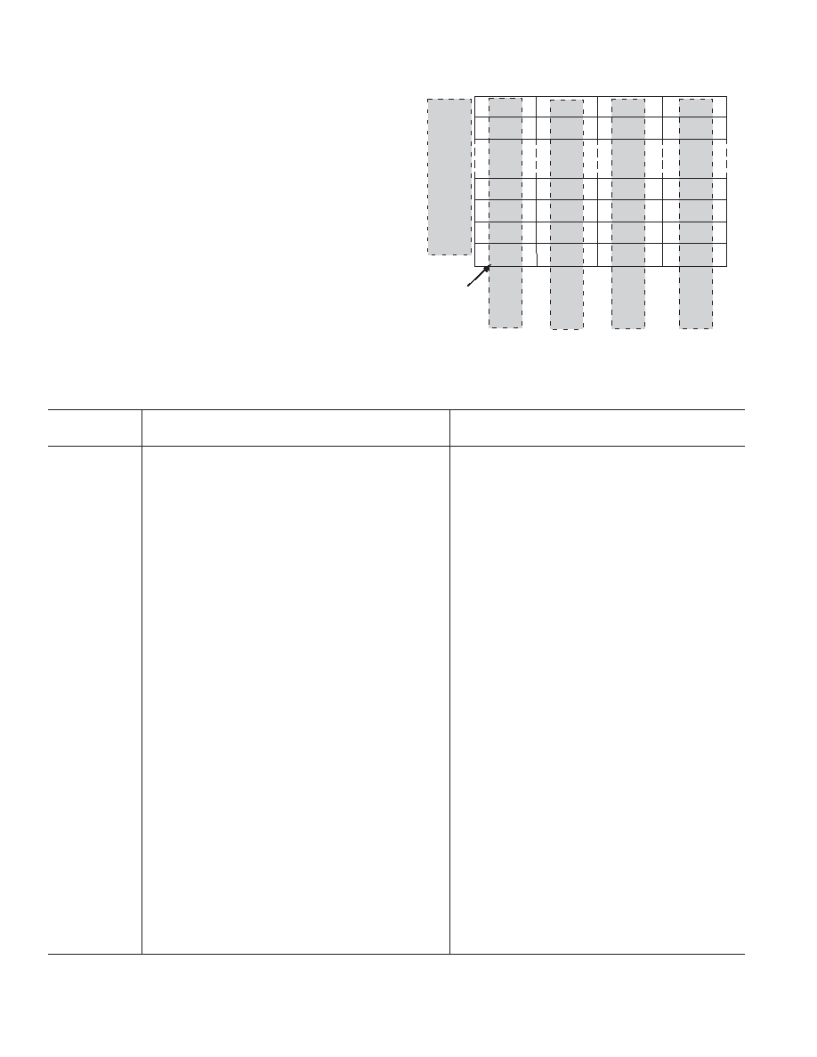
A block diagram of the SFR interface to the Flash/EE data
memory array is shown in Figure 20.
ECON—Flash/EE Memory Control SFR
Programming of either the Flash/EE data memory or the Flash/EE
program memory is done through the Flash/EE Memory Control
SFR (ECON).This SFR allows the user to read, write, erase, or
verify the 4 Kbytes of Flash/EE data memory or the 56 Kbytes of
Flash/EE program memory.
BYTE 1
(0000H)
EDATA1
SF
R
BYTE 1
(0004H)
BYTE 1
(0008H)
BYTE 1
(000CH)
BYTE 1
(0FF8H)
BYTE 1
(0FFCH)
BYTE 2
(0001H)
EDATA2
SF
R
BYTE 2
(0005H)
BYTE 2
(0009H)
BYTE 2
(000DH)
BYTE 2
(0FF9H)
BYTE 2
(0FFDH)
BYTE 3
(0002H)
EDATA3
SF
R
BYTE 3
(0006H)
BYTE 3
(000AH)
BYTE 3
(000EH)
BYTE 3
(0FFAH)
BYTE 3
(0FFEH)
BYTE 4
(0003H)
EDATA4
SF
R
BYTE 4
(0007H)
BYTE 4
(000BH)
BYTE 4
(000FH)
BYTE 4
(0FFBH)
BYTE 4
(0FFFH)
01H
00H
02H
03H
3FEH
3FFH
PAGE
ADDRESS
(E
ADRH/L
)
BYTE
ADDRESSES
ARE GIVEN IN
BRACKETS
Figure 20. Flash/EE Data Memory Control and Configuration
Table XIV. ECON—Flash/EE Memory Commands
Command Description
ECON Value
(Normal Mode) (Power-On Default)
(ULOAD Mode)
01H
Results in four bytes in the Flash/EE data memory,
Not Implemented. Use the MOVC instruction.
READ
addressed by the page address EADRH/L, being read
into EDATA 1 to 4.
02H
Results in four bytes in EDATA1–A4 being written to the Results in bytes 0–255 of internal XRAM being written
WRITE
Flash/EE data memory, at the page address given by
to the 256 bytes of Flash/EE program memory at the
EADRH/L (0 EADRH/L < 0400H)
page address given by EADRH. (0 EADRH < E0H)
Note:The four bytes in the page being addressed must
Note:The 256 bytes in the page being addressed must
be pre-erased.
03H
Reserved Command
04H
Verifies if the data in EDATA1–4 is contained in the
Not Implemented. Use the MOVC and MOVX
VERIFY
page address given by EADRH/L. A subsequent read
instructions to verify the WRITE in software.
of the ECON SFR will result in a 0 being read if the
verification is valid, or a nonzero value being read
to indicate an invalid verification.
05H
Results in the erase of the 4-bytes page of Flash/EE
Results in the 64-byte page of Flash/EE program
ERASE PAGE
data memory addressed by the page address EADRH/L
memory, addressed by the byte address EADRH/L
being erased. EADRL can equal any of 64 locations
within the page. A new page starts whenever EADRL
is equal to 00H, 40H, 80H, or C0H.
06H
Results in the erase of entire four Kbytes of Flash/EE
Results in the erase of the entire 56 Kbytes of ULOAD
ERASE ALL
data memory.
Flash/EE program memory.
81H
Results in the byte in the Flash/EE data memory,
Not Implemented. Use the MOVC command.
READBYTE
addressed by the byte address EADRH/L, being read
into EDATA1. (0 EADRH/L 0FFFH).
82H
Results in the byte in EDATA1 being written into
WRITEBYTE
Flash/EE data memory, at the byte address EADRH/L.
Flash/EE program memory at the byte address
EADRH/L (0 EADRH/L DFFFH).
0FH
Leaves the ECON instructions to operate on the
Enters Normal mode, directing subsequent ECON
EXULOAD
Flash/EE data memory.
instructions to operate on the Flash/EE data memory.
F0H
Enters ULOAD mode, directing subsequent ECON
Leaves the ECON instructions to operate on the Flash/EE
ULOAD
instructions to operate on the Flash/EE program memory.
program memory.
REV. A
相关PDF资料 |
PDF描述 |
|---|---|
| ADUC843BSZ62-5 | IC ADC 12BIT W/FLASH MCU 52-MQFP |
| ADUC845BCPZ62-5 | IC FLASH MCU W/24BIT ADC 56-CSP |
| ADUC847BCPZ62-5 | IC MCU FLASH W/24BIT ADC 56-CSP |
| ADV202BBCZ-135 | IC CODEC VIDEO 135MHZ 144CSPBGA |
| ADV212BBCZ-115 | IC CODEC VID JPEG 2000 121CSPBGA |
相关代理商/技术参数 |
参数描述 |
|---|---|
| ADUC836BCPZ-REEL | 功能描述:IC MCU 62K FLASH ADC/DAC 56LFCSP RoHS:是 类别:集成电路 (IC) >> 嵌入式 - 微控制器, 系列:MicroConverter® ADuC8xx 标准包装:38 系列:Encore!® XP® 核心处理器:eZ8 芯体尺寸:8-位 速度:5MHz 连通性:IrDA,UART/USART 外围设备:欠压检测/复位,LED,POR,PWM,WDT 输入/输出数:16 程序存储器容量:4KB(4K x 8) 程序存储器类型:闪存 EEPROM 大小:- RAM 容量:1K x 8 电压 - 电源 (Vcc/Vdd):2.7 V ~ 3.6 V 数据转换器:- 振荡器型:内部 工作温度:-40°C ~ 105°C 封装/外壳:20-SOIC(0.295",7.50mm 宽) 包装:管件 其它名称:269-4116Z8F0413SH005EG-ND |
| ADUC836BS | 制造商:Analog Devices 功能描述:MCU 8-bit ADuC8xx 8052 CISC 62KB Flash 3.3V/5V 52-Pin MQFP 制造商:Analog Devices 功能描述:8BIT MCU +16BIT DUAL ADC MQFP52 |
| ADUC836BS | 制造商:Analog Devices 功能描述:IC SEMICONDUCTOR ((NS)) |
| ADUC836BSZ | 功能描述:IC ADC DUAL 16BIT W/MCU 52-MQFP RoHS:是 类别:集成电路 (IC) >> 嵌入式 - 微控制器, 系列:MicroConverter® ADuC8xx 标准包装:250 系列:56F8xxx 核心处理器:56800E 芯体尺寸:16-位 速度:60MHz 连通性:CAN,SCI,SPI 外围设备:POR,PWM,温度传感器,WDT 输入/输出数:21 程序存储器容量:40KB(20K x 16) 程序存储器类型:闪存 EEPROM 大小:- RAM 容量:6K x 16 电压 - 电源 (Vcc/Vdd):2.25 V ~ 3.6 V 数据转换器:A/D 6x12b 振荡器型:内部 工作温度:-40°C ~ 125°C 封装/外壳:48-LQFP 包装:托盘 配用:MC56F8323EVME-ND - BOARD EVALUATION MC56F8323 |
| ADUC841 | 制造商:AD 制造商全称:Analog Devices 功能描述:MicroConverter 12-Bit ADCs and DACs with Embedded High Speed 62-kB Flash MCU |
发布紧急采购,3分钟左右您将得到回复。