参数资料
| 型号: | ADUC836BCPZ |
| 厂商: | Analog Devices Inc |
| 文件页数: | 6/80页 |
| 文件大小: | 0K |
| 描述: | IC MCU 62K FLASH ADC/DAC 56LFCSP |
| 标准包装: | 1 |
| 系列: | MicroConverter® ADuC8xx |
| 核心处理器: | 8052 |
| 芯体尺寸: | 8-位 |
| 速度: | 12.58MHz |
| 连通性: | EBI/EMI,I²C,SPI,UART/USART |
| 外围设备: | POR,PSM,PWM,温度传感器,WDT |
| 输入/输出数: | 34 |
| 程序存储器容量: | 62KB(62K x 8) |
| 程序存储器类型: | 闪存 |
| EEPROM 大小: | 4K x 8 |
| RAM 容量: | 2.25K x 8 |
| 电压 - 电源 (Vcc/Vdd): | 2.7 V ~ 5.25 V |
| 数据转换器: | A/D 7x16b; D/A 1x12b |
| 振荡器型: | 内部 |
| 工作温度: | -40°C ~ 85°C |
| 封装/外壳: | 56-VFQFN 裸露焊盘,CSP |
| 包装: | 托盘 |
第1页第2页第3页第4页第5页当前第6页第7页第8页第9页第10页第11页第12页第13页第14页第15页第16页第17页第18页第19页第20页第21页第22页第23页第24页第25页第26页第27页第28页第29页第30页第31页第32页第33页第34页第35页第36页第37页第38页第39页第40页第41页第42页第43页第44页第45页第46页第47页第48页第49页第50页第51页第52页第53页第54页第55页第56页第57页第58页第59页第60页第61页第62页第63页第64页第65页第66页第67页第68页第69页第70页第71页第72页第73页第74页第75页第76页第77页第78页第79页第80页
ADuC836
–14–
ADuC836
–15–
When accessing the internal XRAM, the P0 and P2 port pins, as
well as the RD and WR strobes, will not be output as per a stan-
dard 8051 MOVX instruction.This allows the user to use these
port pins as standard I/O.
The upper 1792 bytes of the internal XRAM can be configured
to be used as an extended 11-bit stack pointer. By default, the
stack will operate exactly like an 8052 in that it will roll over from
FFH to 00H in the general-purpose RAM. On the ADuC836
however, it is possible (by setting CFG836.7) to enable the 11-bit
extended stack pointer. In this case, the stack will roll over from
FFH in RAM to 0100H in XRAM.The 11-bit stack pointer is
visible in the SP and SPH SFRs.The SP SFR is located at 81H
as with a standard 8052.The SPH SFR is located at B7H.The
3 LSBs of this SFR contain the three extra bits necessary to
extend the 8-bit stack pointer into an 11-bit stack pointer.
UPPER 1792
BYTES OF
ON-CHIP XRAM
(DATA + STACK
FOR EXSP = 1,
DATA ONLY
FOR EXSP = 0)
256 BYTES OF
ON-CHIP DATA
RAM
(DATA +
STACK)
LOWER 256
BYTES OF
ON-CHIP XRAM
(DATA ONLY)
00H
FFH
00H
07FFH
CFG836.7 = 0
CFG836.7 = 1
100H
Figure 4. Extended Stack Pointer Operation
External Data Memory (External XRAM)
Just like a standard 8051 compatible core, the ADuC836 can
access external data memory using a MOVX instruction.The
MOVX instruction automatically outputs the various control
strobes required to access the data memory.
The ADuC836, however, can access up to 16 Mbytes of external
data memory.This is an enhancement of the 64 Kbytes external
data memory space available on a standard 8051 compatible core.
The external data memory is discussed in more detail in the
ADuC836 Hardware Design Considerations section.
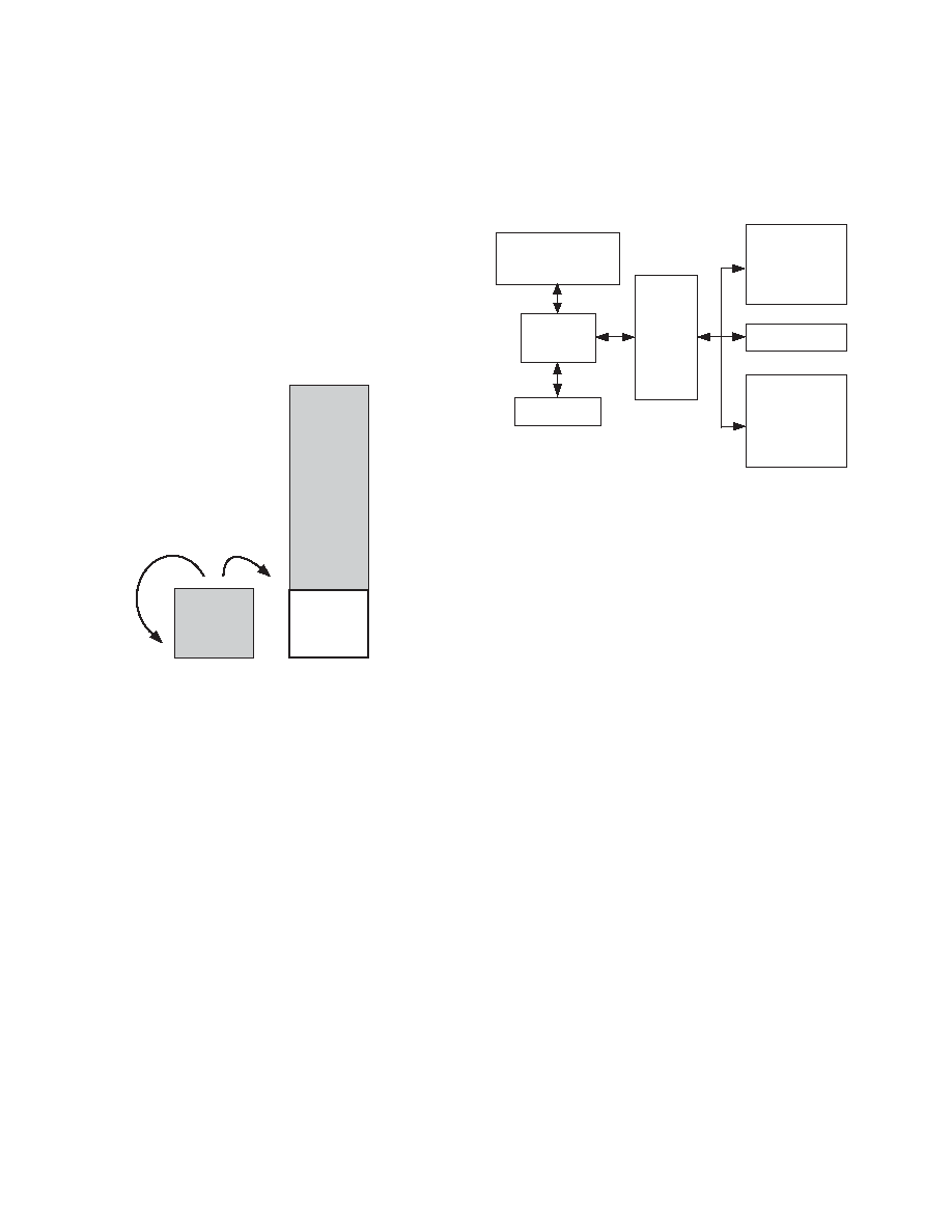
SPECIAL FUNCTION REGISTERS (SFRS)
The SFR space is mapped into the upper 128 bytes of internal
data memory space and accessed by direct addressing only. It
provides an interface between the CPU and all on-chip periph-
erals. A block diagram showing the programming model of the
ADuC836 via the SFR area is shown in Figure 5.
128-BYTE
SPECIAL
FUNCTION
REGISTER
AREA
62 KBYTE ELECTRICALLY
REPROGRAMMABLE
NONVOLATILE FLASH/EE
PROGRAM MEMORY
8051
COMPATIBLE
CORE
OTHER ON-CHIP
PERIPHERALS
TEMP SENSOR
CURRENT SOURCES
12-BIT DAC
SERIAL I/O
WDT, PSM
TIC, PLL
DUAL - ADCs
4 KBYTE
ELECTRICALLY
REPROGRAMMABLE
NONVOLATILE
FLASH/EE DATA
MEMORY
256 BYTES RAM
2K XRAM
Figure 5. Programming Model
All registers, except the Program Counter (PC) and the four
general-purpose register banks, reside in the SFR area.The SFR
registers include control, configuration, and data registers that
provide an interface between the CPU and all on-chip peripherals.
Accumulator SFR (ACC)
ACC is the Accumulator Register, which is used for math
operations including addition, subtraction, integer multiplication,
and division, and Boolean bit manipulations.The mnemonics for
accumulator-specific instructions, refer to the Accumulator as A.
B SFR (B)
The B Register is used with the ACC for multiplication and
division operations. For other instructions, it can be treated as a
general-purpose scratch pad register.
Data Pointer (DPTR)
The Data Pointer is made up of three 8-bit registers, named DPP
(page byte), DPH (high byte), and DPL (low byte).These are
used to provide memory addresses for internal and external code
access and external data access. It may be manipulated as a 16-bit
register (DPTR = DPH, DPL), although INC DPTR instructions
will automatically carry over to DPP, or as three independent 8-bit
registers (DPP, DPH, DPL).
The ADuC836 supports dual data pointers. For more information,
refer to the Dual Data Pointer section.
REV. A
相关PDF资料 |
PDF描述 |
|---|---|
| ADUC843BSZ62-5 | IC ADC 12BIT W/FLASH MCU 52-MQFP |
| ADUC845BCPZ62-5 | IC FLASH MCU W/24BIT ADC 56-CSP |
| ADUC847BCPZ62-5 | IC MCU FLASH W/24BIT ADC 56-CSP |
| ADV202BBCZ-135 | IC CODEC VIDEO 135MHZ 144CSPBGA |
| ADV212BBCZ-115 | IC CODEC VID JPEG 2000 121CSPBGA |
相关代理商/技术参数 |
参数描述 |
|---|---|
| ADUC836BCPZ-REEL | 功能描述:IC MCU 62K FLASH ADC/DAC 56LFCSP RoHS:是 类别:集成电路 (IC) >> 嵌入式 - 微控制器, 系列:MicroConverter® ADuC8xx 标准包装:38 系列:Encore!® XP® 核心处理器:eZ8 芯体尺寸:8-位 速度:5MHz 连通性:IrDA,UART/USART 外围设备:欠压检测/复位,LED,POR,PWM,WDT 输入/输出数:16 程序存储器容量:4KB(4K x 8) 程序存储器类型:闪存 EEPROM 大小:- RAM 容量:1K x 8 电压 - 电源 (Vcc/Vdd):2.7 V ~ 3.6 V 数据转换器:- 振荡器型:内部 工作温度:-40°C ~ 105°C 封装/外壳:20-SOIC(0.295",7.50mm 宽) 包装:管件 其它名称:269-4116Z8F0413SH005EG-ND |
| ADUC836BS | 制造商:Analog Devices 功能描述:MCU 8-bit ADuC8xx 8052 CISC 62KB Flash 3.3V/5V 52-Pin MQFP 制造商:Analog Devices 功能描述:8BIT MCU +16BIT DUAL ADC MQFP52 |
| ADUC836BS | 制造商:Analog Devices 功能描述:IC SEMICONDUCTOR ((NS)) |
| ADUC836BSZ | 功能描述:IC ADC DUAL 16BIT W/MCU 52-MQFP RoHS:是 类别:集成电路 (IC) >> 嵌入式 - 微控制器, 系列:MicroConverter® ADuC8xx 标准包装:250 系列:56F8xxx 核心处理器:56800E 芯体尺寸:16-位 速度:60MHz 连通性:CAN,SCI,SPI 外围设备:POR,PWM,温度传感器,WDT 输入/输出数:21 程序存储器容量:40KB(20K x 16) 程序存储器类型:闪存 EEPROM 大小:- RAM 容量:6K x 16 电压 - 电源 (Vcc/Vdd):2.25 V ~ 3.6 V 数据转换器:A/D 6x12b 振荡器型:内部 工作温度:-40°C ~ 125°C 封装/外壳:48-LQFP 包装:托盘 配用:MC56F8323EVME-ND - BOARD EVALUATION MC56F8323 |
| ADUC841 | 制造商:AD 制造商全称:Analog Devices 功能描述:MicroConverter 12-Bit ADCs and DACs with Embedded High Speed 62-kB Flash MCU |
发布紧急采购,3分钟左右您将得到回复。