参数资料
| 型号: | ADUC836BCPZ |
| 厂商: | Analog Devices Inc |
| 文件页数: | 29/80页 |
| 文件大小: | 0K |
| 描述: | IC MCU 62K FLASH ADC/DAC 56LFCSP |
| 标准包装: | 1 |
| 系列: | MicroConverter® ADuC8xx |
| 核心处理器: | 8052 |
| 芯体尺寸: | 8-位 |
| 速度: | 12.58MHz |
| 连通性: | EBI/EMI,I²C,SPI,UART/USART |
| 外围设备: | POR,PSM,PWM,温度传感器,WDT |
| 输入/输出数: | 34 |
| 程序存储器容量: | 62KB(62K x 8) |
| 程序存储器类型: | 闪存 |
| EEPROM 大小: | 4K x 8 |
| RAM 容量: | 2.25K x 8 |
| 电压 - 电源 (Vcc/Vdd): | 2.7 V ~ 5.25 V |
| 数据转换器: | A/D 7x16b; D/A 1x12b |
| 振荡器型: | 内部 |
| 工作温度: | -40°C ~ 85°C |
| 封装/外壳: | 56-VFQFN 裸露焊盘,CSP |
| 包装: | 托盘 |
第1页第2页第3页第4页第5页第6页第7页第8页第9页第10页第11页第12页第13页第14页第15页第16页第17页第18页第19页第20页第21页第22页第23页第24页第25页第26页第27页第28页当前第29页第30页第31页第32页第33页第34页第35页第36页第37页第38页第39页第40页第41页第42页第43页第44页第45页第46页第47页第48页第49页第50页第51页第52页第53页第54页第55页第56页第57页第58页第59页第60页第61页第62页第63页第64页第65页第66页第67页第68页第69页第70页第71页第72页第73页第74页第75页第76页第77页第78页第79页第80页
ADuC836
–34–
ADuC836
–35–
VDD
VDD–50mV
VDD–100mV
100mV
50mV
0mV
000H
FFFH
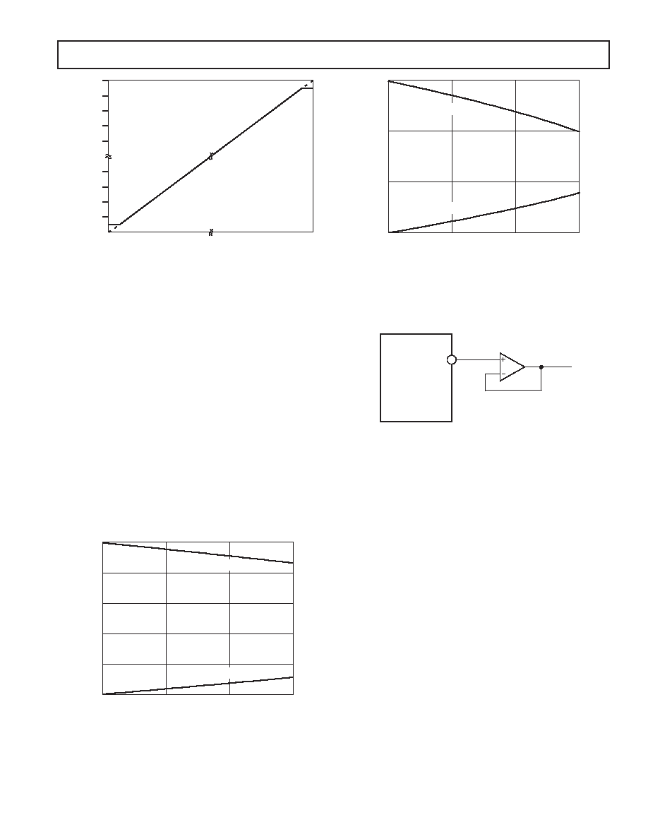
Figure 22. Endpoint Nonlinearities Due to
Amplifier Saturation
Note that Figure 22 represents a transfer function in 0-to-VDD mode
only. In 0-to-VREF mode (with VREF < VDD), the lower nonlinearity
would be similar, but the upper portion of the transfer function
would follow the “ideal” line right to the end, showing no signs of
endpoint linearity errors.
The endpoint nonlinearities conceptually illustrated in Figure 22
get worse as a function of output loading. Most of the ADuC836
data sheet specifications assume a 10 k resistive load to ground
at the DAC output. As the output is forced to source or sink more
current, the nonlinear regions at the top or bottom (respectively)
of Figure 22 become larger.With larger current demands, this
can significantly limit output voltage swing. Figures 23 and 24
illustrate this behavior. It should be noted that the upper trace in
each of these figures is valid only for an output range selection of
0-to-AVDD. In 0-to-VREF mode, DAC loading will not cause high
side voltage drops as long as the reference voltage remains below
the upper trace in the corresponding figure. For example, if AVDD
= 3V andVREF = 2.5V, the high side voltage will not be affected by
loads less than 5 mA. But somewhere around 7 mA, the upper curve
in Figure 24 drops below 2.5 V (VREF), indicating that at these
higher currents, the output will not be capable of reaching VREF.
SOURCE/SINK CURRENT – mA
5
0
5
10
15
OUTPUT
VOLTAGE
–
V
4
3
2
1
0
DAC LOADED WITH 0000H
DAC LOADED WITH 0FFFH
Figure 23. Source and Sink Current Capability
with VREF = AVDD = 5 V
SOURCE/SINK CURRENT – mA
4
0
5
10
15
OUTPUT
VOLTAGE
–
V
3
1
0
DAC LOADED WITH 0000H
DAC LOADED WITH 0FFFH
Figure 24. Source and Sink Current Capability with
VREF = VDD = 3 V
For larger loads, the current drive capability may not be sufficient
To increase the source and sink current capability of the DAC, an
external buffer should be added, as shown in Figure 25.
ADuC836
12
Figure 25. Buffering the DAC Output
The DAC output buffer also features a high impedance disable func-
tion. In the chip’s default power-on state, the DAC is disabled and
its output is in a high impedance state (or “three-state”) where
they remain inactive until enabled in software.
This means that if a zero output is desired during power-up or
power-down transient conditions, a pull-down resistor must be
added to each DAC output. Assuming this resistor is in place, the
DAC output will remain at ground potential whenever the DAC
is disabled.
REV. A
相关PDF资料 |
PDF描述 |
|---|---|
| ADUC843BSZ62-5 | IC ADC 12BIT W/FLASH MCU 52-MQFP |
| ADUC845BCPZ62-5 | IC FLASH MCU W/24BIT ADC 56-CSP |
| ADUC847BCPZ62-5 | IC MCU FLASH W/24BIT ADC 56-CSP |
| ADV202BBCZ-135 | IC CODEC VIDEO 135MHZ 144CSPBGA |
| ADV212BBCZ-115 | IC CODEC VID JPEG 2000 121CSPBGA |
相关代理商/技术参数 |
参数描述 |
|---|---|
| ADUC836BCPZ-REEL | 功能描述:IC MCU 62K FLASH ADC/DAC 56LFCSP RoHS:是 类别:集成电路 (IC) >> 嵌入式 - 微控制器, 系列:MicroConverter® ADuC8xx 标准包装:38 系列:Encore!® XP® 核心处理器:eZ8 芯体尺寸:8-位 速度:5MHz 连通性:IrDA,UART/USART 外围设备:欠压检测/复位,LED,POR,PWM,WDT 输入/输出数:16 程序存储器容量:4KB(4K x 8) 程序存储器类型:闪存 EEPROM 大小:- RAM 容量:1K x 8 电压 - 电源 (Vcc/Vdd):2.7 V ~ 3.6 V 数据转换器:- 振荡器型:内部 工作温度:-40°C ~ 105°C 封装/外壳:20-SOIC(0.295",7.50mm 宽) 包装:管件 其它名称:269-4116Z8F0413SH005EG-ND |
| ADUC836BS | 制造商:Analog Devices 功能描述:MCU 8-bit ADuC8xx 8052 CISC 62KB Flash 3.3V/5V 52-Pin MQFP 制造商:Analog Devices 功能描述:8BIT MCU +16BIT DUAL ADC MQFP52 |
| ADUC836BS | 制造商:Analog Devices 功能描述:IC SEMICONDUCTOR ((NS)) |
| ADUC836BSZ | 功能描述:IC ADC DUAL 16BIT W/MCU 52-MQFP RoHS:是 类别:集成电路 (IC) >> 嵌入式 - 微控制器, 系列:MicroConverter® ADuC8xx 标准包装:250 系列:56F8xxx 核心处理器:56800E 芯体尺寸:16-位 速度:60MHz 连通性:CAN,SCI,SPI 外围设备:POR,PWM,温度传感器,WDT 输入/输出数:21 程序存储器容量:40KB(20K x 16) 程序存储器类型:闪存 EEPROM 大小:- RAM 容量:6K x 16 电压 - 电源 (Vcc/Vdd):2.25 V ~ 3.6 V 数据转换器:A/D 6x12b 振荡器型:内部 工作温度:-40°C ~ 125°C 封装/外壳:48-LQFP 包装:托盘 配用:MC56F8323EVME-ND - BOARD EVALUATION MC56F8323 |
| ADUC841 | 制造商:AD 制造商全称:Analog Devices 功能描述:MicroConverter 12-Bit ADCs and DACs with Embedded High Speed 62-kB Flash MCU |
发布紧急采购,3分钟左右您将得到回复。