- 您现在的位置:买卖IC网 > PDF目录1900 > ADV3002BSTZ-RL (Analog Devices Inc)IC SWITCH HDMI/DVI 4:1 80-LQFP PDF资料下载
参数资料
| 型号: | ADV3002BSTZ-RL |
| 厂商: | Analog Devices Inc |
| 文件页数: | 1/28页 |
| 文件大小: | 0K |
| 描述: | IC SWITCH HDMI/DVI 4:1 80-LQFP |
| 产品变化通告: | Marking Change 25/Mar/2009 |
| 标准包装: | 1,000 |
| 功能: | 开关 |
| 电路: | 1 x 4:1 |
| 电压电源: | 单电源 |
| 电压 - 电源,单路/双路(±): | 3 V ~ 3.6 V |
| 工作温度: | 0°C ~ 85°C |
| 安装类型: | 表面贴装 |
| 封装/外壳: | 80-LQFP |
| 供应商设备封装: | 80-LQFP(14x14) |
| 包装: | 带卷 (TR) |
当前第1页第2页第3页第4页第5页第6页第7页第8页第9页第10页第11页第12页第13页第14页第15页第16页第17页第18页第19页第20页第21页第22页第23页第24页第25页第26页第27页第28页
4:1 HDMI/DVI Switch with Equalization,
DDC/CEC Buffers and EDID Replication
Data Sheet
Rev. B
Information furnished by Analog Devices is believed to be accurate and reliable. However, no
responsibilityisassumedbyAnalogDevicesforitsuse,norforanyinfringementsofpatentsorother
rightsofthirdpartiesthatmayresultfromitsuse.Specificationssubjecttochangewithoutnotice.No
license is granted by implication or otherwise under any patent or patent rights of Analog Devices.
Trademarksandregisteredtrademarksarethepropertyoftheirrespectiveowners.
One Technology Way, P.O. Box 9106, Norwood, MA 02062-9106, U.S.A.
Tel: 781.329.4700
Fax: 781.461.3113
2008–2012 Analog Devices, Inc. All rights reserved.
FEATURES
4 inputs, 1 output HDMI/DVI links
±8 kV ESD protection on input pins
HDMI 1.4a receive and transmit compliant
Supports 250 Mbps to 2.25 Gbps data rates and beyond
Supports 25 MHz to 225 MHz pixel clocks and beyond
Fully buffered unidirectional inputs/outputs
Switchable 50 on-chip input terminations with manual
or automatic control on channel switch
Equalized inputs with low added jitter compensate for
more than 20 meters of HDMI cable at 2.25 Gbps
Loss of signal (LOS) detect circuit on TMDS clock
Output disable feature for reduced power dissipation
Bidirectional DDC buffers (SDA and SCL)
EDID replication reduces component count, while enabling
simultaneous access to all HDMI sources
5 V combiner provides power to EDID replicator and CEC
buffer when local system power is off
Bidirectional buffered CEC line with integrated pull-up
resistors (26 k)
Hot plug detect pulse low on channel switch with
programmable pulse width or direct manual control
Standards compatible: HDMI, DVI, HDCP, I2C
80-lead, 14 mm × 14 mm LQFP RoHS-compliant package
APPLICATIONS
Advanced television (HDTV) sets
Projectors
A/V receivers
Set-top boxes
GENERAL DESCRIPTION
The ADV3002 is a complete HDMI/DVI link switch featuring
equalized transition minimized differential signaling (TMDS)
inputs, ideal for systems with long cable runs. The ADV3002
includes bidirectional buffering for the DDC bus and CEC line,
with integrated pull-up resistors for the CEC line. Additionally,
the ADV3002 includes an EDID replication function that enables
one EDID EEPROM to be shared for all four HDMI ports.
The ADV3002 is provided in a space-saving, 80-lead LQFP
surface-mount, Pb-free plastic package and is specified to
operate over the 0°C to 85°C temperature range.
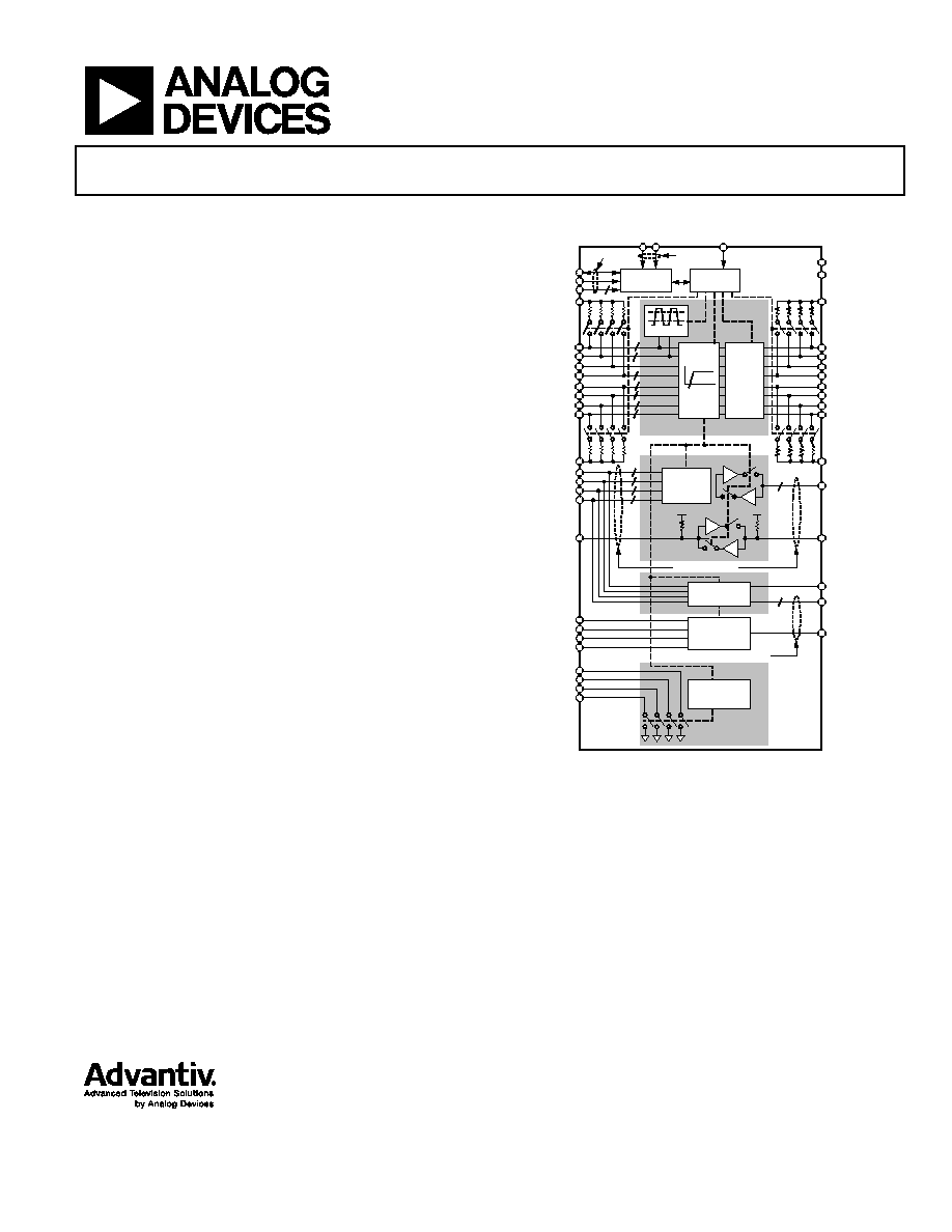
FUNCTIONAL BLOCK DIAGRAM
SERIAL
I2C_SDA
I2C_SCL
I2C_ADDR[1:0]
AVCC
CEC_IN
IN_x_CLK+
IN_x_CLK–
IN_x_DATA2+
IN_x_DATA2–
IN_x_DATA1+
IN_x_DATA1–
IN_x_DATA0+
IN_x_DATA0–
DDC_xxx_A
DDC_xxx_B
DDC_xxx_C
DDC_xxx_D
P5V_A
P5V_B
P5V_C
P5V_D
HPD_A
HPD_B
HPD_C
HPD_D
HOT PLUG DETECT
EDID
DDC/CEC
TMDS
EDID EEPROM INTERFACE
ADV3002
4
2
4
2
4
+
–
+
–
+
–
+
–
+
–
+
–
+
–
+
–
AVCC
AVEE
OUT_CLK+
OUT_CLK–
OUT_DATA2+
OUT_DATA2–
OUT_DATA1+
OUT_DATA1–
OUT_DATA0+
OUT_DATA0–
DDC_SCL_COM,
DDC_SDA_COM
CEC_OUT
EDID_ENABLE
EDID_SCL,
EDID_SDA
AMUXVCC
BIDIRECTIONAL
SEL[1:0] TX_EN
RESETB
CONFIG
INTERFACE
CONTROL
LOGIC
LOS
EQ
SWITCH
CORE
SWITCH
CORE
3.3V
REPLICATOR
CONTROL
5V
COMBINER
07905-
001
PARALLEL
HPD
CONTROL
Figure 1.
PRODUCT HIGHLIGHTS
1. Input cable equalizer enables use of long cables at the input.
For a 24 AWG cable, the ADV3002 compensates for more
than 20 meters at data rates of up to 2.25 Gbps.
2. Auxiliary multiplexer isolates and buffers the DDC bus and
the CEC line, increasing total system capacitance limit.
3. EDID replication eliminates the need for multiple EDID
EEPROMs. EDID can be loaded from a single external
EEPROM or from a system microcontroller.
4. 5 V power combiner powers the EDID replicator and CEC
buffer when local system power is off.
5. Integrated hot plug detect pulse low on channel switch
with programmable pulse width or direct manual control.
相关PDF资料 |
PDF描述 |
|---|---|
| ADV3003ACPZ-R7 | IC EQUALZR HDMI/DVI TMDS 40LFCSP |
| ADV3200ASWZ | IC CROSSPOINT SWIT 32X32 176LQFP |
| ADV3203ASWZ | IC CROSSPOINT SWIT 32X16 176LQFP |
| ADV3205JSTZ | IC CROSSPOINT SWIT 16X16 100LQFP |
| ADV3220ACPZ-R7 | IC MULTIPLEXER 2:1 16LFCSP |
相关代理商/技术参数 |
参数描述 |
|---|---|
| ADV3002-EVALZ | 制造商:AD 制造商全称:Analog Devices 功能描述:4:1 HDMI/DVI Switch with Equalization, DDC/CEC Buffers and EDID Replication |
| ADV3002XSTZ | 功能描述:IC SWITCH HDMI/DVI 4:1 80LQFP 制造商:analog devices inc. 系列:- 包装:托盘 零件状态:上次购买时间 类型:视频开关 应用:HDTV,投影仪,机顶盒 安装类型:- 封装/外壳:- 供应商器件封装:- 标准包装:1 |
| ADV3002XSTZ-RL | 功能描述:IC SWITCH HDMI/DVI 4:1 80LQFP 制造商:analog devices inc. 系列:- 包装:带卷(TR) 零件状态:上次购买时间 类型:视频开关 应用:HDTV,投影仪,机顶盒 安装类型:- 封装/外壳:- 供应商器件封装:- 标准包装:1 |
| ADV3003 | 制造商:AD 制造商全称:Analog Devices 功能描述:HDMI/DVI TMDS Equalizer |
| ADV3003ACPZ | 功能描述:IC EQUALZR HDMI/DVI TMDS 40LFCSP RoHS:是 类别:集成电路 (IC) >> 接口 - 专用 系列:- 特色产品:NXP - I2C Interface 标准包装:1 系列:- 应用:2 通道 I²C 多路复用器 接口:I²C,SM 总线 电源电压:2.3 V ~ 5.5 V 封装/外壳:16-TSSOP(0.173",4.40mm 宽) 供应商设备封装:16-TSSOP 包装:剪切带 (CT) 安装类型:表面贴装 产品目录页面:825 (CN2011-ZH PDF) 其它名称:568-1854-1 |
发布紧急采购,3分钟左右您将得到回复。